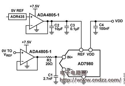
The ADA4805-1 is a high speed voltage feedback rail-to-rail output amplifier with excellent quiescent current performance down to 495 μA, making it ideal for low power, high resolution data conversion systems. Despite its low power consumption, the amplifier still provides excellent overall performance. The device features a high bandwidth of 105 MHz (gain of 1), a high slew rate of 160 V/μs, and a low input offset voltage of up to 125 μV.
The shutdown pin allows further reduction of the quiescent supply current to 3 μA. For power-sensitive applications, the shutdown mode provides a very high-speed turn-on time of 3 μs from off to full turn-off (output is 16 bits). This allows the user to turn off the amplifier between two ADC samples for dynamic power management.
The amplifier is fabricated on Analog Devices' proprietary ultra-fast complementary bipolar (XFCB) process with low voltage and low current noise performance (5.9 nV/√Hz, 0.6 pA/√Hz). Supporting a wide supply voltage range of ±1.5 V to ±5 V and a single supply of 3 V and 5 V, the ADA4805-1 is ideal for high speed, low power instrumentation.
ADA4805-1 features:
1. Low input offset voltage: 125 μV (max)
2. Low input offset voltage drift - 0.2 μV/°C (typ.), -1.5 μV/°C (max)
3. Ultra-low supply current: 495 μA per amplifier
4, wide power supply voltage range: 3 V to 10 V
5, high speed performance - −3 dB bandwidth: 105 MHz, - slew rate: 160 V / μs
ADA4805-1 application:
1, high resolution, high precision ADC driver
2, battery powered instrumentation
3, micro power active filter
4, portable POS terminal
5, active RFID card reader
6, photomultiplier tube
7, ADC reference buffer
Internal function diagram of ADA4805-1:

Figure 1: Internal function diagram of ADA4805-1
Typical application of ADA4805-1:

Figure 2: Typical application of ADA4805-1
The ADA4805-1/ADA4805-2 are high speed voltage feedback, rail-to-rail output amplifiers with very low quiescent current of 500 μA, making them ideal for low power, high resolution data conversion systems. Despite the low power consumption, these devices still provide excellent overall performance. They have a high bandwidth of 105 MHz, a high slew rate of 160 V/μs, and a low input offset voltage of 125 μV at +1 gain. The shutdown pin allows the quiescent supply current to be further reduced to 2.9 μA. For power sensitive applications, the shutdown mode provides an extremely fast turn-on time of 3 μs. It shuts down the amplifier between two ADC samples, allowing the user to dynamically manage amplifier power consumption
ADA4805-1 Chinese Data Sheet: Download Now
ADA4805-2 Chinese Data Sheet: Download Now
More source code and PCB schematic:
Brake Disc
Brake Disc,Car Brake Disc,Automobile Brake Disc,Auto Brake Disc
Zhoushan Shenying Filter Manufacture Co., Ltd. , https://www.renkenfilter.com