The digital instrument cluster integrates a variety of vehicle and safety information in a more cost-effective and more flexible configuration, motivating drivers to focus more on driving vehicles. Drivers no longer have to look down on the central control, rushing to find music buttons, making phone calls, inquiring about driving directions or looking around to see dead ends. These innovative inventions will become reality, helping drivers to concentrate and focus on safe driving. These new advancements offer many exciting new options, but they also require designers to uncover innovative solutions that deliver critical performance while ensuring long-term reliability while controlling costs. This article will first focus on some of the limitations of automotive design/reliability, and then evaluate the digital instrument cluster architecture and how the storage subsystem's trade-offs affect future project performance, reliability, and cost.
This article refers to the address: http://
The Challenge of Digital Instrument Group Design The digital instrument cluster must support high-performance real-time processing requirements (like existing consumer-grade display platforms) while significantly increasing the long-term reliability of the design. OEMs (original equipment manufacturers), Tier 1 suppliers and customers in the automotive market will never see display failures as small problems that often occur on consumer phones or PCs. The new digital instrument cluster needs to create an easy-to-use, interference-free information environment that promotes safe driving. These products must ensure excellent performance levels and long-term reliable operation while withstanding harsh and harsh working conditions (eg , -40 to +105 ° C extreme temperature range). These harsh requirements in the automotive industry for environmental, safety and quality have led to a very long development cycle, and sometimes it takes three years or more to develop a vehicle display technology.
The planning, design, and verification process for automotive design is extremely systematic in order to identify and eliminate operational or reliability issues. In this process, the electronic component suppliers selected by automotive designers usually develop products using strict quality design methods such as TS16949, and comply with the AEC-Q100 standard of the Automotive Electronics Council (AEC).
Once a supplier introduces a mass production system, the component supplier must continuously monitor its internal and external reliability and, if necessary, take corrective action to ensure that the parts per million (dppm) of defective parts are reduced to zero. OEMs and Tier 1 suppliers also want their supply base to provide long-term product support and availability; once a car embedded system is deployed, it will cost a lot to stop, and sometimes it is impossible to support a short life cycle. Re-verify a design with the part. In some cases, the cost of revalidation can be as high as hundreds of thousands of dollars.
The increasing use of graphical content in digital instrument clusters has led to more sophisticated information display systems, which not only require an increase in performance levels, but must also reliably accomplish the basic goal of notifying drivers of basic vehicle and safety information. For example, a digital instrument cluster must be able to provide vehicle status information in a near-instant manner after the vehicle is launched, typically displaying important gearbox gear information on the TFT screen in less than one second (ie, P, R, D, 1 , 2, 3). This requires the instrument cluster to be activated in an instant, and to achieve this, the designer needs to carefully study the performance at the critical system and component level. Even seemingly simple information that provides a warning of insufficient tire pressure before the vehicle is launched can proactively reduce potential safety issues in advance.
The transition from instrumentation to digital systems is exciting, but as noted above, this transition also increases complexity, and designers have to find innovative solutions to meet demanding system requirements such as real-time display performance and long-term height. Reliable and drastically cut costs.
We will look at how to provide this basic information in a reliable and cost-effective manner.
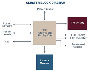
Figure 1 is a schematic diagram of an advanced digital instrument cluster. The vehicle's central system-on-chip (SOC) acquires input data through its communication network and internal or external memory and outputs it to the TFT display. The digital instrument cluster uses a system architecture similar to many consumer-grade high-performance display platforms.

Figure 1 Schematic diagram of the advanced digital instrument cluster
Both automotive and consumer display platforms require large amounts of memory to support their vast digital content; today's automotive designs, 3D graphics content, 32-bit color, high resolution, and large display screens have resulted in storage densities of 2 Gb.
To create a rich display system, the content typically includes large character sets, multiple fonts, graphic images, and multi-language extension support. The digital instrument cluster frame buffer is generated and displayed according to industry standard techniques. The SOC display controller renders a frame on the system display, and the SOC/Graphics Engine accesses the internal or external memory to acquire, process, and save the next set of data in the frame buffer for subsequent display. Today's SOCs require high bandwidth access to reliable code and data residing in external memory, ensuring fast system startup and high-speed real-time processing.
The choice of memory architecture and design implementation of the digital instrument cluster architecture and memory subsystem can affect the performance level and reliability of embedded systems. We will evaluate several memory architectures to illustrate some of the performance/cost trade-offs that can be achieved with current technology. First, Figure 2 briefly outlines the standard code-mapped memory architecture, which is typically used in high-performance embedded display systems.

Figure 2 Standard Code Mapping Memory Architecture
The system controller or general purpose processing unit (GPU) is highly integrated, including the graphics engine, display controller, not only provides limited capacity RAM and flash memory options, but also provides an external memory interface to meet the digital instrument cluster for high Performance and high density memory requirements. External memory is divided into two standard products: DRAM and flash memory. The startup of an embedded system is divided into three main steps: first, the code/data is mapped from flash to DRAM, then the processor, DRAM, and other key components are initialized, and finally the application is executed. Once the code is started, useful information is displayed. This architecture has several key features. The high-speed access capabilities of SOC/DRAM can improve the performance of real-time processing functions. The initial system startup time depends mainly on the time of mapping and initialization, while the mapping time depends on the SOC/Flash access bandwidth and the data density transferred from flash to DRAM.
As mentioned earlier, the high-end digital instrument cluster must provide current vehicle status in near-instantaneous form after the vehicle is launched. The gear position information (ie P, R, D, 1, 2, 3) usually needs to be displayed on the TFT screen within one second. This requires flash memory to support high-speed access, ultra-high storage density and long-term data integrity to meet basic design and quality requirements, while also requiring procurement responsibility to ensure long-term supply stability.
Currently, flash vendors offer a variety of non-volatile memory (NVM) technologies, the two most widely used of which are NOR and NAND flash. Both have different performance characteristics in various aspects, such as accessibility, reliability, product life cycle and cost. Automotive SOCs typically support multiple interface configurations to access external parallel and serial NOR flash, while NAND flash interfaces are increasingly being widely supported.
Note that a dynamic variable on the SOC NAND interface determines the level of ECC support required, especially considering that NAND is rapidly transitioning to lithography. On the NOR side, page mode and synchronous NOR flash will continue to meet the stringent requirements of the automotive industry. For example, the new high-end digital instrument clusters such as the Chevrolet Volt's E-Flex instrument cluster are based on Freescale's MPC5121e SOC and Spansion's S29GL512N flash. Spansion GL page read access technology supports high-speed read access with data throughput rates of up to 80MB/s, which fully meets the needs of the Volt E-Flex instrument cluster, ensuring that it displays the gearbox within one second of the car's start-up Bit (ie P, R, D, 1, 2, 3).
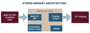
The constant innovation of automotive chipset and flash memory suppliers has spawned a cost-effective new hybrid digital instrument cluster architecture (see Figure 3). System controllers (Freescale Spectrum) and flash memory (Spansion Multi I/O SPI) optimize the TFT display architecture to provide a more cost-effective entry-level instrument cluster solution. The system controller executes code through the embedded flash and simultaneously loads graphics data from the external flash using the high bandwidth multiple I/O SPI protocol. The graphic data is processed and saved in the internal frame buffer and then directly displayed on the TFT screen. This bold and innovative hybrid architecture eliminates the need for external DRAM memory, not only to meet system performance and reliability requirements, but also to optimize cost.

Figure 3 hybrid memory architecture
Note that this application architecture requires hundreds of millions of read cycles and therefore affects the availability of technologies such as NAND. Currently, when NAND devices are used for applications with medium and high read cycles, more bit interference errors occur.
The new multi-I/O SPI communication protocol can be used for data transfer between the system controller and external SPI flash. The Multi-I/O SPI is based on the popular Serial Peripheral Interface (SPI) and its access performance is configured to support 1 to 4 data connections. This feature can increase the accessibility of SPI from less than 10Mb/s to 40Mb/s. Automotive chipset and flash memory vendors such as Freescale and Spansion offer a wide range of standard products, enabling designers to take advantage of the improved access bandwidth of multiple I/O SPIs for better cost control while creating high-performance digital Instrument cluster. In some cases, two quad I/O SPIs can be used to support continuous throughput rates of up to 80 MB/s.
Spansion's multi-I/O SPI FL flash family still supports low pin count serial interfaces and supports higher read bandwidths than current multi-pin count flash devices. The Spansion SPI FL Series is also designed to meet medium to high storage densities and long-term data integrity requirements, maintaining normal operation up to 105 ° C while meeting AEC-Q100 standards.
we offer 38kv Power Pole and 30m High Mast.
Yixing Futao Metal Structural Unit Co. Ltd. is com manded of Jiangsu Futao Group.
Power Tower, Power Pole, Electric Power Pole, Power Transmission Line Pole,35ft Power Pole,38kv Power Pole
YIXING FUTAO METAL COMPONENT UNIT CO.,LTD , http://www.chinasteelpole.com