TOP1 car alarm system module circuit based on fingerprint recognition
The main working principle: After the vehicle owner stops the fire, the anti-theft device enters the locked state. At this time, if the car key is not in the ON position, fingerprint recognition cannot be performed; only when the car key is in the ON position, the fingerprint recognition can be used to unlock the immobilizer and automatically ignite. In the locked state, the oil circuit and circuit of the car are cut off, and the car key cannot be ignited; if the connection between the fingerprint acquisition module and the control box is forcibly cut, or the fingerprint is forcibly ignited by the car key, the car will pass the horn, Flashing lights and wireless communication network alarms. Insert the password key in the locked state to enter the unlocked state, and perform fingerprint registration/delete, mobile number setting and emergency ignition through the keypad according to the LCD and voice prompts.
USB interface circuit
The USB interface circuit is mainly realized by the file management control chip CH376T. The CH376T supports the USB device mode and the USB host mode, and has built-in basic firmware of the USB communication protocol, firmware for processing the dedicated communication protocol of the MassStorage mass storage device, and communication interface firmware of the SD card. , FAT16 and FAT32 and FAT12 file system management firmware, support common USB storage devices and SD cards. The CH376T supports two communication interfaces: SPI interface and asynchronous serial port. This design uses SPI interface to communicate with MCU data. The circuit connection is shown in Figure 2. Serial data input SDI, output SDO and clock SCK are respectively connected to SPI1_MOSI, SPI1_MISO and SPI1_SCK of STM32F103VC, interrupt request output terminal INT is connected to PC0, and chip select terminal SCS is controlled by PA1. The RESET in the figure is the system reset signal, and the crystal oscillator Y1 selects 12 MHz. When the car mainly performs fingerprint registration/deletion or emergency ignition, the password key (U disk) is connected to J1 to read the password information.

Voice circuit
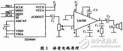
The schematic diagram of the voice circuit is shown in Figure 3. It consists of the ISD company's voice chip ISD4004-16 and National Semiconductor's audio power amplifier LM386. ISD4004 -16 recording and playback time is 16 min (segmentable), it uses CMOS technology, single power supply 3 V operation, including oscillator, anti-aliasing filter, smoothing filter, audio amplifier, automatic squelch and high density Level flash storage display. It has a built-in microcontroller SPI bus serial communication interface. Analog voice data can be written directly to a single location without the need for A/D or D/A conversion. The ISD voice circuit has many advantages such as natural sound quality, convenient use, single-chip storage, repeated recording and playback, low power consumption, and power failure. The LM386 operates over a wide voltage range with adjustable voltage gain. It has low power consumption, adjustable voltage supply, large power supply voltage range, few external components and low total harmonic distortion. In this design, the STM32F103VC transmits voice information to the ISD4004 via SPI2. In Figure 3, V1 and V2 are connected to the +3.3 V and +12 V power supplies via a triode. The triode is switched on and off by the PCI1 and PCI2 of the STM32F103VC. The triode is turned on to the ISD4004 only when a voice prompt is required. Powered by the LM386.

ARM-based optical fingerprint identification system circuit module
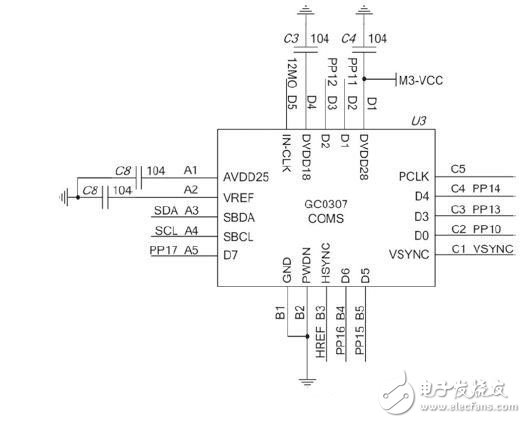
The entire system design constitutes an integrated optical fingerprint recognition module. The module design adopts the principle of optical dark background imaging, and adds a special living body detection chip to solve the problem of residual fingerprint misidentification and rubber false fingerprint while solving the dry finger effect. The figure shows the schematic diagram of the application circuit of the optical GC0307 CMOS image acquisition chip. This CMOS image acquisition chip is a built-in component of a high-precision, low-power, micro-volume, high-performance camera that combines CMOS image sensors for high-quality VGA images with highly integrated image processors, embedded power supplies, and high-quality The lens group is combined to output a JPEG image or image video stream, supports 8/10 digit digital transmission of JPEG images and YCbCr interface, providing a complete imaging solution.

The CMOS image acquisition core function output serial data pin, clock signal pin, reset pin, serial bus pin, etc. are all connected to the GPIO port of the STM32F205RE, and the image information acquired by the CMOS chip is read through the GPIO port analog timing. . Since the STM32F205RE's GPIO port can operate at 120 MHz, the timing can be simulated very accurately and efficiently. The original image of the measured 640 & TImes; 480 can be acquired into the main processor STM32F205RE for image processing at 10 frames/s.
Wall Power Socket,Multi Plug Outlet,Wall Power Outlet,Electric Wall Socket
Wenzhou Niuniu Electric Co., Ltd. , https://www.anmuxisocket.com