3D image information processing has always been a hot and difficult point in the field of image and video processing. At present, there are not many mature 3D information processing systems at home and abroad. Existing systems mainly rely on high-performance general-purpose PCs to complete image acquisition, preprocessing, reconstruction, configuration, etc. Handling work at the bottom and top. The data volume of 3D image processing is extremely large, and the calculation is complicated. It is difficult to achieve real-time requirements simply by relying on a general-purpose PC, which cannot meet the current high-speed 3D image processing applications.
In this system, FPGA is used to implement the underlying signal preprocessing algorithm, which has a large amount of data and high processing speed, but the algorithm structure is relatively simple, which can take into account both speed and flexibility. The high-level processing algorithm has less data volume and complex algorithm structure, which can be realized by DSP with fast operation speed, flexible addressing mode and powerful communication mechanism [1, 4].
1 Three-dimensional image processing system
1.1 Hardware system composition
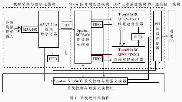
The system consists of five modules, as shown in Figure 1.

The system information processing flow is shown in Figure 2. The multi-channel analog video signal collected by the CCD camera is selected by MAX440 as required, and then sent to the analog-to-digital video converter SAA7111A to convert the analog full TV signal CVBS output by the camera into a digital video signal; the video signal then flows into the image pre-processor Spartan XC3S400 After preprocessing of extracting the center color line, extracting the laser marking line and the object contour line, it is distributed to two TS201s for the calculation of calibration parameters, coordinate calculation, 3D reconstruction, data fusion and the core operation of 3D configuration; finally the DXF The file data is transferred to the PC via the PCI interface to complete the final processing such as three-dimensional image conversion and display; the logical connection and control of the entire system and part of the data exchange are completed by another FPGA [1].

In terms of architecture design, the FPGA processor uses a SIMD structure. Under the control signal generated by a control unit, the three algorithms in the data path run in parallel. Because the system requires high processing speed, pipeline technology is used in the data path to increase the speed. In addition, many large-capacity high-speed FIFOs are used for image storage in this system to reduce address lines and simplify control.
1.2 Processor chip
In order to meet the requirements of rapid processing of large amounts of data in the system, the three core chips are the latest high-performance products. Their hardware characteristics bring great convenience to the system design, and their excellent computing performance can ensure the rapid real-time performance of the system.
The FPGA chip adopts the XC3S400 of the Spartan3 series recently adopted by Xilinx, which adopts the 90nm process. This series of chips is by far the most advanced process, the price is lower, and the platform-level programmable logic device with the most I / O pins per unit cost. The internal clock frequency of the XC3S400 chip can reach 326MHz, the signal swing is 1.14V and 3.45V, the I / O port supports a data transfer rate of 622Mbps, with high-performance SelectRAM internal memory, up to 4 digital clock manager modules and 8 global clocks Multiplexed buffer.
The DSP adopts the latest TIgerSHARC ADSP TS201 based on parallel processing design with massive on-chip RAM. Its internal integrated RAM capacity is up to 24Mbit, and the core speed is up to 600MHz. Built-in dual operation modules, each containing an ALU, MUL, 64bit shift register, 32 32bit register groups and a 128bit communication logic unit, related data alignment buffer; double integer ALU, each with independent register group, provide Data addressing and pointer operation; four 128-bit wide internal buses, each connected to six 4Mbit internal memory blocks; provides connection to host processor, multiprocessor space, off-chip memory mapped peripherals, external SRAM and SDRAM External port; 14-channel DMA controller; 4 full duplex low voltage differential signal input Link Port; with on-chip arbitration bus for seamless connection of multiple DSPs.
The digitizer uses the SAA7111A analog-to-digital converter, Philips' Enhanced Video Input Processor (EVIP). The product is widely used in personal video, multimedia, digital TV, videophone, image processing, real-time monitoring and other fields. The analog 3.3V CMOS process analog video front end and digital video encoder can decode PAL / TSC / ECAM video signals It is a variety of digital video formats compatible with CCIR-601. It supports CVBS or S-Video video signals from TV or VTR signal sources. The maximum image resolution can reach 720 × 576. It supports 24-bit true color and can be passed through a serial bus. Dynamic configuration
The working mode and various parameters of SAA7111A analog-to-digital converter.
2 Module design
2.1 Video capture and digitization module
Because the analog camera collects the composite video signal (CVBS) of the PAL system, it must be digitized before the subsequent digital video processing can be started. The video acquisition and digitization module mainly includes a video multiplexer MAX440, a SAA7111A, an I2C interface controller PCF8584 and some connection logic. MAX440 is used to quickly switch analog video streams from different analog inputs. The SAA7111A analog-to-digital converter is the core of the module. It captures analog video and digitizes it into a 720 × 576 RGB (8, 8, 8) true color signal format In digital video, the RGB true color signal output is 16 bits, in which the high byte and low byte data periods are 74ns and 37ns respectively, that is, the frequency of the low byte is twice that of the high byte. In this way, it is necessary to use a trigger and two clock signals of 13.5MHz and 27MHz to convert the input data format to a 24-bit RGB true color signal with a period of 74ns. In addition, it also provides the necessary clock for the entire hardware system And synchronization signal; PCI interface controller configures and controls SAA7111A through PCF8584, and the connection logic is implemented by FPGA.
2.2 FPGA image preprocessing module
Pre-processing extracts a very small amount of information useful for 3D reconstruction from huge video information and sends it to the DSP for post-processing. This module includes the main processing FPGA chip and high-speed FIFO. It is responsible for collecting video signals in real time and preprocessing the collected uncompressed video information, including extracting the laser center line, extracting the contour line, and extracting the center color line.
In order to improve the overall performance of video capture, it is more important to provide adjacent laser and non-laser frames for preprocessing. The laser-free frames must be temporarily stored through the video frame buffer. The buffer is composed of 3 pieces of AverLogic AL422B and some connection logic implemented by FPGA; when the front end module outputs no laser frame, SA7111A controls 3 pieces of AL422B write operation and stores it in FIFO; when the current end outputs a laser frame, after The video processing module at the end controls the three AL422Bs to perform a read operation, and reads out the non-laser frame data temporarily stored therein. The preprocessing FPGA subtracts the read laser-free frames and laser frames. The output also uses three sets of buffers to temporarily store laser spline data, target contour data and image centerline data; all modules are controlled by a synchronous clock, which uses the LLC2 signal generated by the SAA7111A analog-to-digital converter. In order to improve the speed of the system, the calculation process with complex algorithm and long time-consuming is pipelined.
2.3 DSP 3D reconstruction module
In order to cope with the need for complex and high-speed calculation of large data volume of three-dimensional images, two TIgerSHARC 201 chips are used in parallel three-dimensional reconstruction operation. The control FPGA assigns tasks to the images to be processed by the two DSPs. The DSP combines the data stored in the FIFO with the preprocessing FPGA and the processing parameters given by the PCI bus to perform calibration parameter calculation, coordinate calculation, three-dimensional reconstruction and configuration. Due to the bus arbitration mechanism integrated within TS201, dual DSPs can be seamlessly connected, greatly reducing the design difficulty of multi-DSP coordination work. The connection between DSPs depends on the full-duplex LinkPort it has, which uses LVDS (low-level differential signal) to input data. The link port can work independently or simultaneously, and latch data on the rising and falling edges of the clock. The link clock frequency can be the same as the processor core, up to 500MHz, and each link can complete 500Mbps unidirectional data transmission. The four LinkPorts of each DSP together have a maximum transmission rate of 4.0Gbps. The connection is short and simple, no additional auxiliary circuit is needed, and the signal distortion caused by the long connection can be effectively prevented. LinkPort transmission protocol is completed by the control FPGA.
2.4 PCI communication interface module
According to the speed transmission requirements of the three-dimensional information acquisition system, the PCI interface is used to complete the information interaction between the system and the general PC. The PCI interface controller is the control center and data exchange center of the hardware part. It receives commands and data from the device driver, configures and controls the various modules of the system to coordinate work, and complete system tasks; it is also responsible for collecting and processing The data is transferred to the general-purpose PC through the PCI bus. This system uses PLX's 32bit / 33MHz PCI9030 as the interface chip, and serial EEPROM-FM93CS56L electrically erasable read-only memory to save PCI9030 configuration information.
2.5 System control and data exchange module
The control unit controls the data processing unit and input data format conversion unit of the processor and all FIFO memories, and cooperates with the preprocessing FPGA to complete the LinkPort protocol of the DSP. Due to the pipeline processing in the data processing unit, special attention should be paid to the delay of the fixed cycle generated by the pipeline in the design of the control unit. The number of delay cycles is equal to the number of stages of the corresponding pipeline. The control unit is also connected to the PCI interface and receives information such as control signals and background thresholds from the host computer. The control FPGA is also a bridge for the exchange of images and information between the SAA7111A, PCI interface and DSP, providing the required parameters and data information.
3 Software design and implementation
3.1 Image preprocessing algorithm
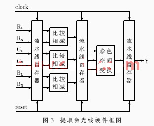
As shown in Figure 3, the implementation of the laser band preprocessing algorithm [2] is: Since the laser frame and the non-laser frame are generated alternately in sequence, first save a frame with a laser frame, and the next frame, that is, no laser frame When it arrives, the points of the same rows and columns of the saved laser frame and the current no laser frame are subtracted, and then the brightness is extracted, and the processed data is stored in the target cache.

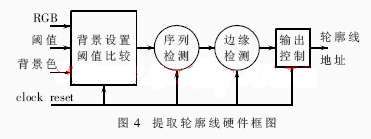
As shown in Figure 4, the algorithm for extracting contour lines is divided into three parts [3]. First, the calculation and comparison module compares the value of the input pixel with the pre-calculated threshold to determine whether it is the target pixel; then uses a sequence to detect The module performs one-dimensional scale filtering to remove some noise points; then through an edge detection module, the first target pixel of each row is extracted as the left edge point of the target; after completion, the column address data corresponding to this point is stored Target cache. In some cases, the edge point may not be detected in the entire line, and at this time, 0 is stored in the target cache as an identifier of no edge point.

The algorithm for extracting the centerline is relatively simple. It only needs to control the write permission signal of the target cache, so that the RGB data can only be written to the target cache at the center point of each line.
3.2 3D reconstruction and configuration
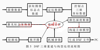
As shown in Figure 5, the high-speed DSP combines the laser marking line, contour line and center color line data obtained from the preprocessing information with the source digitized image for three-dimensional reconstruction. Firstly, the system calibration data is calculated based on the acquired image mark point data combined with the control point 3D coordinate data; secondly, the developed image of the outer surface of the object is calculated based on the contour line, and then the coordinate points in the image are combined with the expanded data and mechanical parameters Calculate, give the data set, output the depth data file; finally fuse the data of multiple scans, the discrete point configuration into a volume model (or stereo color model), and generate DXF, STL and other data files from the model to the PC , Use the back-end processing software for display [3].

3.3 Algorithm implementation
The image preprocessing algorithm design was successfully implemented using Verilog HDL in Xilinx's ISE8.1 integrated compilation environment; the FPGA development process will not be repeated.
The DSP three-dimensional reconstruction algorithm has been successfully implemented in the Visual DSP ++ environment of Analog Devices using C language [4]. The algorithm implementation steps are as follows: ①Program the algorithm in C language. ② Use Visual DSP ++ compiler to compile the source program into the target file. ③ According to the generated target file, analyze the results and the structure of the source program and optimize the source code. ④Apply TIgerSHARC 201 evaluation board to evaluate the operation time. ⑤ Repeat the above steps until reaching the real-time requirements of the system, and finally download to the target board.
The entire system runs stably online, meets the design requirements, and has good real-time performance.
Real-time three-dimensional image information processing is difficult to use integrated circuits because of its large data volume, high speed requirements, and complex processing. The three-dimensional image processing system with FPGA + DSP as the core architecture of the latest high-performance processor studied in this paper has carefully designed the hardware implementation of the algorithm, making full use of the advantages of the two processors. Experiments show that the system has good performance and is of great significance for real-time network-based 3D scanning applications, such as 3D fax, remote machining of machines, rapid prototyping and virtual reality.
references
[1] LEI HAIJUN, LI DEHUA. High-Speed ​​aerial image processing system based on DSP, In neural nerwork and distributed processing, Proceedings of SPIE Vol. 4555, 2001: 131-136
[2] Lei Haijun, Li Dehua, Wang Jianyong, etc. A fast detection method of structured light fringe center [J]. Journal of Huazhong University of Science and Technology, 2003, 31 (1): 74-76.
[3] Jin Gang. Research on Theory and Technology of 3D Information Acquisition in 3D Scanner [D]. Doctoral Dissertation of Huazhong University of Science and Technology, 2002, (3)
[4] Lu Haidong, Wu Mingzan. Design of wavelet image processing system based on FPGA + DSP structure [J], Application of Electronic Technology, 2006, (3) 93-95
Water-cooled capacitor is supercapacitor is a capacitor with a capacity of thousands of farads.According to the principle of capacitor, capacitance depends on the distance between the electrode and electrode surface area, in order to get such a large capacitance, as far as possible to narrow the distance between the super capacitor electrode, electrode surface area increased, therefore, through the theory of electric double layer and porous activated carbon electrode.
Water-Cooled Capacitor,Water-Cooled Power Capacitor,Water-Cooled Electric Heat Capacitor,Water-Cooled Electric Heating Capacitor
YANGZHOU POSITIONING TECH CO., LTD. , https://www.yzpst.com