The CAN (Controller Area Network) bus is the controller area network. It is one of the field buses. It is a bus serial communication network designed by Bosch of Germany for the monitoring and control system of automobiles. It is suitable for industrial process control equipment and monitoring equipment. Interconnection. It is a multi-master serial communication bus. The basic design specification requires high bit rate, high immunity to electromagnetic interference, and can detect any errors generated. Mainly used in automotive electrical control systems, elevator control systems, safety monitoring systems, medical equipment, textile machinery, ship transportation and other aspects. CAN has the following main features: 1 low cost; 2 long-distance transmission (up to lOKm); 3 high-speed data transmission rate (up to 1Mbit/s); 4 can receive or block the message according to the ID of the message; Reliable error handling and error detection mechanism; 6 After the information sent is destroyed, it can be automatically resent; 7 nodes have the function of automatically exiting the bus in case of serious error.
CAN interface circuit of embedded system
CAN interface hardware modules based on arm7 architecture embedded system include Samsung's embedded microprocessor S3C44BOX and Philips' CAN controller chip SJAl000 and CAN bus transceiver PCA82C250 ($0.6186). The 8KB Cache and Samsung S3C44BOX microprocessors are Samsung's cost-effective and high-performance microcontroller solutions for handheld devices and general applications. They use the arm7TDMI CPU core and operate at 66 MHz. In order to reduce the total system cost and reduce peripheral devices, the chip also integrates the following components: external memory controller, LCD controller, 4 DMA channels, 2 channel asynchronous UART unit, 1 synchronous serial port (SIO), 1 multi-master 12C bus controller, 1 I Is bus controller, 5-channel PWM timer and one internal timer, 71 general-purpose I/O ports, 8 external interrupt sources, real-time clock, 8-channel 10-bit ADC Wait.
CAN bus controller
The CAN bus controller uses SJAl000 from Philips. SJAl000 is a stand-alone controller for Controller Area Network (CAN) in automotive and general industrial environments. It is an alternative to the PHILIPS Semiconductor PCA82C200 CAN Controller (BasicCAN). Moreover, it adds a new working mode (PeliCAN) that supports the CAN2.0B protocol with many new features. SJA1000 ($2.8080) is a new generation of CAN controller with the following features: 1 pin compatible and electrically compatible with PCA82C200 independent CAN controller; 2SJA1000 has two working modes: basic CAN mode (BASIC CAN) and enhanced CAN mode (PELI) CAN), support CAN2.0A/B protocol; 3 support 11-bit and 29-bit ID at the same time, bit rate up to 1M, with bus arbitration function; 4 extended receive buffer (64 bytes, first in first out FIFO), enhanced The ambient temperature range (-40-+125 ° C); 5 error detection and error correction capabilities; 6 support for hot swap.
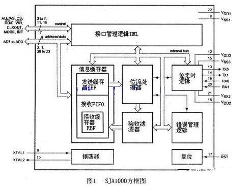
The SJA1000 block diagram is shown in Figure 1. The interface management logic IML is responsible for connecting an external host controller, which may be a microcontroller or any other controller. The interface management logic IML receives commands from the microcontroller, allocates a control information buffer to the transmit buffer TBF, receive buffers RBF0 and RBF1, and provides interrupt and status information to the microcontroller. The Transmit Buffer TBF consists of a 10-byte memory location that stores the messages that are written by the microcontroller and will be sent to the CAN bus network. Receive buffers 0 and 1 (RBF0, RBF1) are each composed of 10 bytes, alternately storing messages received from the bus. When one buffer is allocated to the CPU, the bit stream processor can write to the other. The bit stream processor is a sequencer that controls the flow of data between the transmit buffer and the receive buffer (parallel data) and the CAN bus (serial data). The bit timing logic synchronizes the SJA1000 to the bit stream on the CAN bus. The acceptance filter supports filtering of 11-bit and 29-bit identifiers, and all received messages are accepted by the acceptance filter and stored in the receive FIFO. The error management logic completes the error definition in accordance with the CAN protocol.

CAN bus transceiver
The CAN bus transceiver uses the PCA82C250 product from Philips. The CAN bus transceiver is the interface between the CAN protocol controller and the physical bus. The device provides differential transmission capability to the bus and provides differential reception capability to the CAN controller. It has strong immunity to electromagnetic interference (EMI). At least 110 nodes can be attached.
CAN interface circuit of embedded system
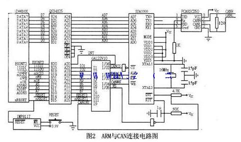
2 is a CAN interface circuit diagram of the embedded microprocessor S3C44BOX. As shown, ARM and SJA1000 are connected in a bus mode. Since the ARM signal is 3.3 volts and the CAN bus controller is at 5 volts, level shifting is required between all signals. In this example, QS34X245 is used. 0.7575) as a level shifting chip. The QS34X245 is an 80-pin dual-in-line chip that combines level shifting (5V to 3.3V) and a bus switch and isolation device. The QS34X245 provides a set of 32-bit high-speed CMOS-compatible bus switches. When the output enable terminal OEn (n is 1 to 4) is low, the switch is turned on, and the bus A and bus B can be connected. When the output enable terminal OEn is When high, the switch is off and bus A is isolated from bus B. OE1 controls the lower 8 bits of bus A and bus B (ie, A7 to A0 and B7 to B0), OE2 controls A15 to A8 and B15 to B8, OE3 controls A23 to A16 and B23 to B16, and OE4 controls A31 to A24 and B31 to B24. Since the ARM bus is not multiplexed and the SJA1000 bus is multiplexed, the address latch signal ALE must be generated by logic, which in this example is generated by the chip GAL22V10. The chip selection and read/write signals of the SJA1000 use the arm bus signal, and the ALE signal is generated by the GAL by the read/write signal and the address signal. When writing the SJA1000 register, first write data to an address of the bus. As an address, the read/write signal is invalid, and the ALE change generates a latch signal; then another address is written, and the read/write signal is valid as data. The above logic is completely generated by the GAL. In addition, the CAN bus needs to add a 120 ohm resistor to the two wires.

When controlling the CAN bus, first initialize each register to set communication parameters (such as mode, bit rate, acceptance code, mask code, field length, bus timing, output mode, etc.), and the BASIC CAN mode control segment has a total of 10 bytes. When sending data, first set the command register, then write the sent message to the send buffer, and finally set the request to send, and send it by SJAl000. The receiver receives the information through the query status register, reads the receive buffer, and then releases the receive buffer.
Semiconductor Stud Devices are mainly used for rectifying and switching
By using the unidirectional conductivity of the diode, alternating direction alternating current can be transformed into pulse direct current in a single direction.
Applications for Medium power switching and DC power supplies.
Semiconductor Stud Devices,Stud Mounted Semiconductor Devices,Stud Mounted Power Semiconductor Device,Ir Semiconductor Stud Thyristor
YANGZHOU POSITIONING TECH CO., LTD. , https://www.cnpositioning.com