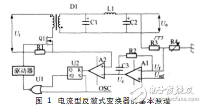
The single-ended flyback switching power supply uses a well-stabilized dual-loop feedback (output DC voltage isolated sampling feedback outer loop and primary coil magnetizing peak current sampling feedback inner loop) control system, which can pass the switching power supply PWM (pulse width) The modulator) quickly adjusts the pulse duty cycle to effectively adjust the output voltage of the previous cycle and the peak current of the primary coil in each cycle to achieve a stable output voltage. The most important feature of this feedback control circuit is that it has a faster dynamic response speed when the input voltage and load current change greatly, automatically limits the load current, and the compensation circuit is simple. The flyback circuit is adapted to a small power switching power supply, and its schematic diagram is shown in FIG.
The following is an analysis of the operation of current-mode PWM under ideal no-load conditions. Compared with the voltage type PWM, the current type PWM adds an inductor current feedback link.
In the figure: A1 is the error amplifier; A2 is the current detection comparator; U2 is the RS flip-flop; Uf is the feedback sample of the output voltage Uo, and the feedback sample and the reference voltage Uref generate the error signal Ue through the error amplifier A1 (the signal is also A2) Compare the clamp voltage).
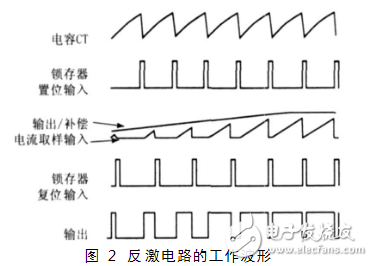
When the FET Q1 is turned on, the inductor current iL increases linearly with the slope Ui/L, L is the primary inductance of T1, and the inductor current is sampled by the sense resistor R1, u1=R1iL, and the sampled voltage is sent to the current detection comparison. Comparator A2 is compared with Ue from the error amplifier. When u1"Ue, A2 outputs a high level and is sent to the reset terminal of RS flip-flop U2. Then the two input NAND gate U1 outputs a low level and turns off Q1; When the clock outputs a high level, the NOR gate U1 always outputs a low level, and the PWM is blocked. When the oscillator output clock falls, both inputs of the NOR gate U1 are low, and Q1 is turned on.
Therefore, it can be seen from the above analysis that the rising edge of the current-mode PWM signal is determined by the falling edge of the oscillator clock signal, and the falling edge of the PWM is determined by the trapping signal of the inductor current and the error signal from the error amplifier. Its working sequence is shown in Figure 2.
The single-ended flyback switching power supply is characterized by the periodic turn-on and turn-off of the main switch. When the switch tube is turned on, the energy is continuously stored in the primary side coil of the transformer; when the switch tube is turned off, the transformer supplies the inductor energy stored in the primary side coil to the load through the rectifier diode until the next pulse arrives, starting a new cycle.
The pulse transformer in the switching power supply plays a very important role: one is to realize the electric field-magnetic field-electric field energy conversion, to provide a stable DC voltage for the load; the other is to realize the transformer function, through the primary winding of the pulse transformer and more The secondary winding can output multiple different DC voltage values ​​to provide DC power for different circuit units. Thirdly, it can realize the electrical isolation of the traditional power transformer, isolate the hot ground from the cold ground, avoid electric shock accidents, and ensure the user terminal. Safety.
Three working modes and output waveforms of single-ended flyback circuitsThe flyback power supply has three modes of operation: continuous operation mode, intermittent operation mode, and critical continuous operation mode.
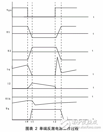
(1) Continuous working modeWhen the single-ended flyback power supply is fully loaded or reloaded, the duty ratio of the switch is large, and the MOS transistor is turned on when the secondary side diode is not turned off. In the working process, there is no case where the primary and secondary currents are simultaneously 0, that is, the continuous mode is operated. Its working waveform is shown in Figure 2.
The work process is analyzed as follows:
1) Before the time t0, the switch tube is in the on state, the primary current rises, the transformer stores energy, the primary side voltage is positive, the secondary side voltage is negative, the capacitor C1 slowly discharges to R1, and the C1 voltage decreases. Primary current secondary current
2) t0~t1 stage. At time t0, turn off the switch. (a) The primary current decreases rapidly, and the decreasing speed is Vin/Lm, the secondary diode is turned on, and the secondary current is rapidly increased; (b) the current on the primary side is reduced, and the primary voltage is reduced. Small, the secondary side voltage rises, both of which pass 0 at the same time, then each reaches the minimum and maximum values, the secondary voltage is 2V, the primary voltage is) / / (2psNNV. (c) due to the junction capacitance of the MOS tube, Therefore, the voltage on it cannot be abrupt, it is zero voltage shutdown. The voltage drop of the MOS tube is) / (2psinNNVV+; (d) In this process, since the current on the leakage inductance cannot be abrupt, the C1 is charged, C1 is no longer Decrease, there is an increasing trend.
3) Time t1~t2. In this process, (a) the primary secondary voltage and the MOS tube voltage drop remain substantially unchanged; (b) since U1 reaches a negative maximum at time t1, its voltage is higher than the C1 voltage, so C1 is charged and quickly reaches Maximum value; (c) Since the transformer energy is released, the secondary current is slowly reduced.
4) Time t2~t3. Turn off the MOS tube at time t2. (a) The primary side voltage rises rapidly, the secondary side voltage begins to decrease, and the maximum and minimum values ​​are reached at time t3. (b) The current has a large peak in the process, and the cause of the spike has two aspects: first, since the secondary current is forced to turn off when the current is not reduced to 0, the reflection is generated to the primary side; Second, since the primary inductance voltage changes rapidly in this process, it can be seen from dtdiLU/⋅= that the current increases rapidly with the change of voltage, and the peak current reaches the minimum value at time t3;
5) After time t3, the MOS tube junction capacitor discharges, and is quickly turned on completely, and its working process is the same as before t0.
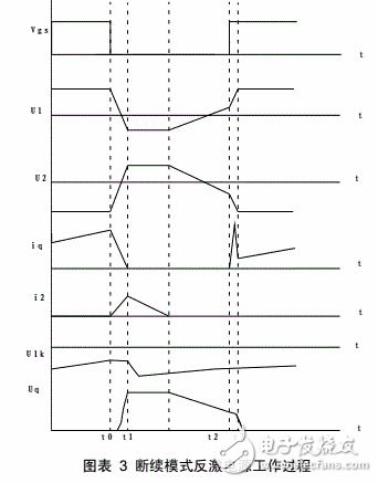
(2) Intermittent working modeThe flyback power supply may operate in discontinuous mode at no load or light load. When the load is no load or light load, the duty ratio of the switch is small. After the switch is turned off, the current of the secondary side decreases linearly and decreases to 0 before the switch is turned on. At this time, the current of the primary and secondary sides is 0, and the flyback power supply works. Intermittent work mode.
The working process in the single-ended flyback power supply intermittent mode is shown in Figure 3.
The working process is as follows:
1) The working state is the same as the continuous mode before t0 and t0~t1;
2) t1~t2 time. This time period can be divided into two time periods. (a) The secondary current decreases linearly, the stored energy of the transformer is released to the secondary side, the primary voltage is negative, the size is) / / (2psNNV, the secondary voltage is V2, the voltage drop across the MOS tube is) / ( 2psinNNVV+; (b) After the secondary current drops to 0, the primary voltage starts to rise linearly because there is no clamping of the secondary side mapping voltage. Since the current is almost 0, it is known by CtiUUinq/) (∆⋅=−∆, voltage The change is very slow, the secondary side voltage decreases linearly, and the voltage drop of the MOS tube also decreases as the primary side voltage rises, until the MOS tube is turned on at time t2;
3) t2~t3 time. Since the MOS transistor is turned on, the primary side voltage rises linearly and its slope is minLU/, and the secondary side voltage decreases linearly. The primary inductance voltage changes rapidly in this process. It is known from dtdiLU/â‹…= that the current increases rapidly with the change of voltage, and the peak current reaches the minimum value at time t3;
4) After time t3, the MOS tube junction capacitor discharges and is fully turned on very quickly, and its working process is the same as before t0.
(3) Critical continuous working modeIn the critical continuous industrial attack mode, the operating waveform of the single-ended flyback power supply is shown in Figure 4.
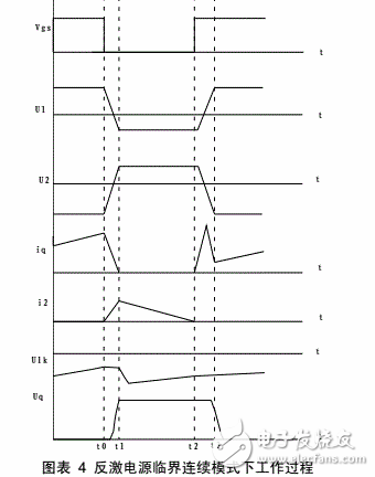
The critical continuous mode of operation is a transition between continuous mode and discontinuous mode, which can be considered as continuous mode analysis and can be analyzed as discontinuous mode.
The working process is basically the same as the continuous mode. There are two differences:
1) At the end of the t1~t2 phase, at the time t2, the secondary current drops to zero and the secondary diode just turns off.
2) The primary current spike in the t2~t3 phase is only caused by the change of the primary side inductor voltage, and is not mapped by the secondary diode. This is consistent with the discontinuous mode.
Shot blasting is a conventional technology for metal surface treatment.As a kind of shot blasting material zinc-based Alloy has wide range of applications with high precision surface treatment,and is safer and more environmentally friendly in use.
Product specification: Ñ„0.3mm~Ñ„1.2mm
Purity: 99.995%min
Product packing: 10-20kgs(spool packing)
30-350kgs(drum packing)
Zinc Shot,Zinc Based Alloy Wire,Zinc Cut Wire Shot,Sand Blasting Zinc Shot
Shaoxing Tianlong Tin Materials Co.,Ltd. , https://www.tianlongspray.com