introduction
PCB Layout is an extremely important step in the process of switching power supply R&D. It is related to whether the switching power supply can work normally, whether the production runs smoothly, and whether the use is safe.

Switching power supply PCB Layout is more complex and difficult than other product PCB layouts. There are many more issues to consider and they are summarized in the following aspects:
First, the circuit requirements
The components in the 1PCB must be the same as the BOM.
The 2 line traces must conform to the schematic diagram. Using the network connection can do this lightly.
3 The width of the line must meet the maximum current requirement and must not be less than 1mm/1A to ensure that the temperature rise of the line does not exceed 70°C. In order to reduce the voltage drop, it is sometimes necessary to widen the width.
4 In order to reduce the voltage drop and loss, tin plating on the strip is optional.
Second, safety regulations
1 The primary side and secondary side circuits should be separated by the isolation band, and the isolation band should be clear and distinct. Relying on the components of the isolation band, the electrical distance should be maintained under the thrust of 10N.
2 The middle of the barrier tape shall be separated by a 1mm screened dashed line, and the DANGER / HIGH VOLTAGE shall be identified in the high pressure zone.
3 Clearances (spatial distance) between circuits:
(1) Primary side communication part:
Fuse before LN≧2..5mm
LN land (PE) ≧ 2. 5mm
After the fuse does not require.
(2) Primary side AC to DC section ≧ 2mm
(3) Primary DC ground to ground 4mm
(4) Primary side to secondary side part 4mm (between primary and secondary side components)
(5) Secondary side:
Voltage less than 100V ≧ 0.5mm
Voltage higher than 100V≧1.0mm
(6) The secondary side of the earth to 1mm
5 Creepage distance between circuits:
(1) Primary AC section:
Fuse before LN≧2..5mm
LN land (PE) ≧ 2. 5mm
After the fuse does not require.
(2) Primary side AC to DC section ≧ 2mm
(3) Primary DC ground to ground 4mm
(4) Primary side to secondary side ≧ 6.4mm
Optocoupler, Y capacitor, slotted when the pitch ≦6.4.
(5) Between the secondary side: When the voltage is lower than 100V, ≧0.5mm; When the voltage is higher than 100V, calculate according to the voltage.
(6) The secondary side of the earth ≧ 2mm.
(7) ≧8mm between transformer secondary sides
5 wire and PCB edge distance should be ≧ 1mm
When the distance between the conductive part on the 6 PCB and the shell is less than 4 mm, a 0.4 mm Mylar sheet should be added.
7PCB must meet flame protection requirements.
III. EMI requirements
1 Primary circuit and secondary circuit are arranged separately.
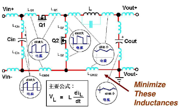
2 AC loop, PFC, PWM loop, rectifier loop, and filter loop The smaller the area surrounded by these four loops is, the better, that is, the requirements:
(1) The power components in each loop are as close as possible to each other.
(2) The power lines (between the two AC lines, between the positive line and the ground line) are close to each other.
3 The control IC should be as close as possible to the MOS tube being controlled.
4 The components around the control IC should be placed as close to the IC as possible, especially the components directly connected to the IC, such as RT, CT resistance capacitors, and the network resistors and capacitors, should be arranged near the IC corresponding PIN. RT, CT to PIN lines should be as short as possible .
5PFC, PWM circuit should be grounded to a single point. The ground of the peripheral component of the IC is connected to the S-pole of the MOS first, and then the S-pole is led to the negative pole of the PFC capacitor.
6 The feedback lines should be as far away as possible from the leads of interference sources (such as PFC inductors, PFC diode leads, MOS transistors), and they must not be routed in close proximity to them.
7 The digital ground should be separated from the simulation ground. The space between ground lines should meet certain requirements.
8 The loop of the bias winding should be directly connected to the negative pole of the PFC capacitor. .
9 Power lines (lines that flow through high currents) should be short and wide to reduce losses, increase the response frequency, and reduce the frequency range of the receiving interference spectrum.
10 In the vicinity of the X capacitor and PFC capacitor pins, the copper strips should be narrowed in order to make full use of the capacitance filtering.
11 Output filter capacitor If necessary, two small capacitors can be used in parallel to reduce ESR.
12PFC MOS and D, PWM MOS heat sinks must be connected once to reduce common-mode interference.
13 The secondary heat sink and transformer outer shield should be connected to the secondary ground.
14 A capacitor should be connected between the primary and secondary side of the transformer or between the DC positive pole and the secondary side ground to provide a discharge shortcut for common mode interference.
15 The inner shield of the transformer should be connected to the primary DC positive pole to suppress the secondary side common mode interference.
16 AC loop should be far away from the PFC, PWM loop to reduce interference from the latter.
17 As far as possible, the upper layer of the double-layer PCB has a wide line, and the ground line should be placed on the upper layer as much as possible.
18 multi-layer PCB application layer as a ground, a layer as a power line, to take full advantage of the decoupling of the inter-layer capacitance, to reduce interference.
IV. Thermal requirements
1 PCB layout should take full account of the mounting attitude and position of the PCB. Under natural heat dissipation conditions, when the PCB is placed vertically, heat-generating inductors and transformers should be placed on top so as not to heat other heat-sensitive components; if it is placed horizontally, heat-sensitive components should also be considered. , Such as small cards, MOS tube, should stay away from inductors, transformers.
2 The selection of heat sinks should consider the direction of heat flow and should be conducive to air convection; when dissipated naturally, the teeth should be upward; when forced air is forced, the teeth should follow the wind direction.
3 Transformers, inductors, rectifiers, and other components that generate large amounts of heat should be placed at the outlet or at the edges so that the heat can be carried directly outside the casing.
4 The direction of the fin teeth is preferably downwind to facilitate convection.
5 If necessary, open the PCB under or near the component to facilitate heat dissipation.
6 Thermal components such as electrolytic capacitors and ICs should be kept away from heat.
7 Components with high temperature, such as transformers, PFC inductors, and components around the filter inductor heat sink should not be too close to avoid burns. Keep temperature-sensitive components away from these parts.
V. Production process and installation requirements
1 Dimensions, installation dimensions, input/output interface must meet the requirements of Spec (supported by the host), and it must be easy to install and use.
2 All components (plug-ins, patches) should use the lead year component library standard package. When self-constructed components are packaged, the size of the holes should ensure that the components can be inserted smoothly. Hole diameter = component leg diameter + 0.3mm.
Between the components and between the components and the heat sink, there should be enough clearance to facilitate the plug and prevent short circuit.
4 All holes including pad holes, via holes, mounting holes, vent holes, and PCB edge are at least 1mm apart.
5 The pitch of the axial components and jumpers should be consistent as much as possible to reduce the component forming and installation tools.
6 compatible component holes should be separated and wired together.
7 Do not use too much PCB expansion coefficient for mounting devices. Otherwise, solder joints will be broken.
8 Small cards should be combined into one large plate, and two sides of the large plate should be left with 5mm bars to pass the tin furnace. Up to 3 rows, separated by V-grooves.
9 Into the direction of the board to be marked.
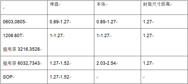
10 Mounting component pads The distance between the body and the body should meet the following requirements:

11 Different types of device dimensions and distances are as follows:
12 Ceramic capacitors larger than 0805, whose direction should be in the direction of the feed plate, (high stress in vertical direction, easily damaged)
13 Do not place the patch within 3mm of the plug nearby to prevent the patch from damaging the patch.
14 The minimum distance between plug pads should be >1mm.
The 15DIP pad can be ovalized to ensure a minimum distance of >0.6mm.
16 All components are >1mm away from the V-CUT.
17 Pluggable and adjustable devices leave enough space for easy plugging or debugging.
18 There should be no components or traces in the area where the installation is prohibited. ∮ 5-12 The following installation holes shall be ∮10-12.
19 Leave some space for the cable to pass through the bent part of the cable, otherwise the component will be bent.
When there are traces below the heat sink, jumpers or components should have a certain height to ensure safety requirements.
21 Assembled pad and trace connections should use tear pads as much as possible.
When there are 22 small cards, there should be a reference point on it.
23 silk screen
(1). Each component, small card, heat sink, and lead-out hole should have a silk-screened label. The label should be consistent with the BOM, and the screen-printing direction should be kept in two directions.
(2). Silk screens cannot be placed on pads, vias, and solder tracks. Silk screens cannot be placed under components (except for high densities).
(3). The polarity of electrolytic capacitors and diodes should be marked. The symbols of TO-220, TO-247 and other devices should ensure that the direction of the plug-in will not be mistaken.
(4). PCB should have a trademark, product model, PCB number / piece number, version, date, location should be eye-catching, size should be moderate.
24 fuses have specifications, warning text.
Insulated Power Cable,Bimetallic Crimp Lugs Cable,Pvc Copper Cable,Cable With Copper Tube Terminal
Taixing Longyi Terminals Co.,Ltd. , https://www.longyiterminals.com