As the SoC baseband chip design scale is highly integrated, the verification cycle will continue to increase, accounting for 70% of the entire development phase [1]. In order to make baseband chip verification more efficient, the current mainstream UVM verification methodology is adopted. The UVM verification methodology [2] was officially launched by Accellera in 2011. The verification platform created not only provides many interfaces available, but the diverse Cadence VIP also provides the necessary components for the UVM environment. Therefore, high-capacity functional verification can be realized, and the simulation verification time is greatly reduced.
The baseband radio frequency interface circuit is a digital serial interface that connects the baseband chip and the radio frequency chip. This digital serial interface not only saves hardware resources, but also enables the baseband to reach a higher uplink and downlink air interface peak transmission rate by carrier aggregation. Due to the complex privatization protocol interface, a suitable verification platform must be built to quickly and comprehensively verify the function of the RF interface circuit. This article will use the UVM verification methodology to verify the baseband RF interface circuit module, the verification method will fully cover all the functional points of the RF transceiver path.
1UVM verification platform
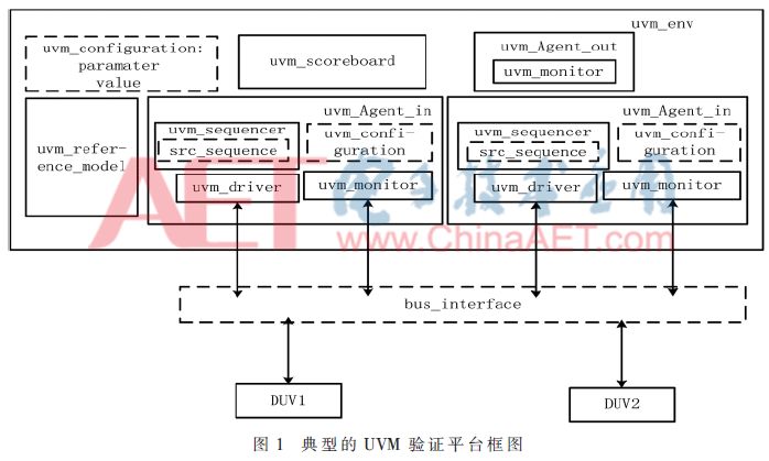
Design Under Verification based on UVM characteristics, based on the System Verilog [3] hardware verification language, calls the various verification components through the UVM library [4], so that the verification work division is clear. This UVM library mainly contains the following parts: First, the hierarchical verification structure. The agent mainly collects modules such as drivers; the driver is responsible for adding the generated excitations to the pins or internals of the DUT according to rules; the monitor detects the internal signals and outputs of the DUV to implement various monitoring operations; The Scoreboard compares the DUV value with the expected value of the Model; the Reference model uses the DUT-related model established by SystemVerilog to output the expected value. Second, the UVM Sequencer [5] provides an arbitration sequence module that causes the driver to obtain a transaction type packet. Third, provide a core of intellectual property (VIP) to ensure rapid integration of components in the UVM environment.
A typical UVM verification platform is shown in Figure 1. In the verification environment, uvm_env contains all the verification components, and the two verification designs are connected to the platform through the bus interface. The verification platform instantiates five modules, two input agent modules, one output agent module, one reference model module and one scoreboard module from the top of env according to the top-down structural specification. The input agent module first configures the verification environment, and then transmits the excitation source to the driver module through the sequencer module. The driver module transmits the data to the slave receiver through the interface, and the monitor can acquire the data signal of the driver to verify the design. The output agent monitor module performs real-time sampling to verify the output signal of the design, and the collected result is placed on the scoreboard module, and compared with the output information of the reference model module, thereby reducing the verification error rate and reducing the verification risk.
2 baseband RF interface circuit module
The baseband radio interface module includes a receive path module and a transmit path module of the radio frequency interface. The baseband RF interface module architecture is shown in Figure 2. The RF interface module uses the AXI standard bus protocol to transmit the slave address and data signals to the configuration module through the X2P bridge. The timing of the receive path is enabled through the GPIO output. The SPI controls the external RF chip by configuring the read/write registers. The receive path status is configured by the receive control register module to turn the RF receive on and off at the configurable TBU time point. The data stream received by the baseband RF interface is buffered by two FIFOs, and the data stream is transferred to the memory in the baseband chip through the AXI host using two sets of DMA. The transmit path process is reciprocal to the receive path process. The transmit status is configured through the transmit control register. The RF transmit is turned on and off at the configurable TBU time point. The data stream of the baseband chip host memory passes through the AXI bus and uses 4 sets of DMA buffers. The four FIFOs are finally sent to the RF chip. During the radio frequency interface receiving and receiving process, after the DMA numbering task is completed, an interrupt is issued, and the interrupt is transmitted to the ARM processor, so that the ARM processor cyclically responds and configures multiple tasks. If the FIFO data is to be re-cached, the FIFO must be cleared, the registers reset at the configurable TBU time point, and the output data is written from the current sample point to the start address of the FIFO.
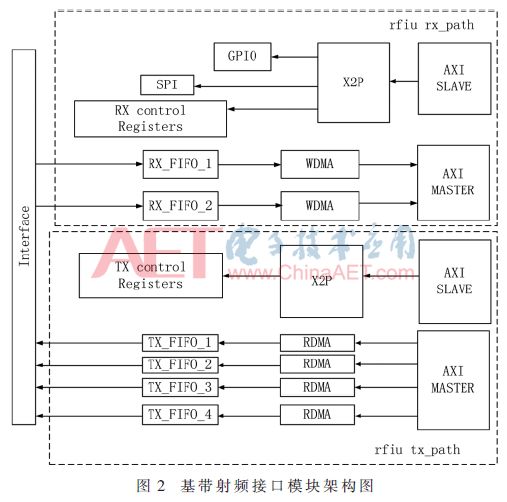
The baseband RF interface uses a multi-mode, multi-bandwidth data interface to support the corresponding interface rate. The CMOS TDD (Complementary Metal Oxide Semiconductor Time Division Duplex) mode uses two sets of 12-bit data lines, and the data transmission uses half-duplex mode, one clock cycle. Dual antenna symbol data can be sent. In CMOS FDD (Complementary Metal Oxide Semiconductor Frequency Division Duplex) mode, the data transfer rate is twice that of CMOS TDD mode data throughput. The LVDS (Low Voltage Differential Signaling) mode data transfer rate is four times the data throughput rate of the CMOS TDD mode.
1Build a UVM-based baseband RF interface circuit verification platform
3.1 baseband RF interface circuit verification process
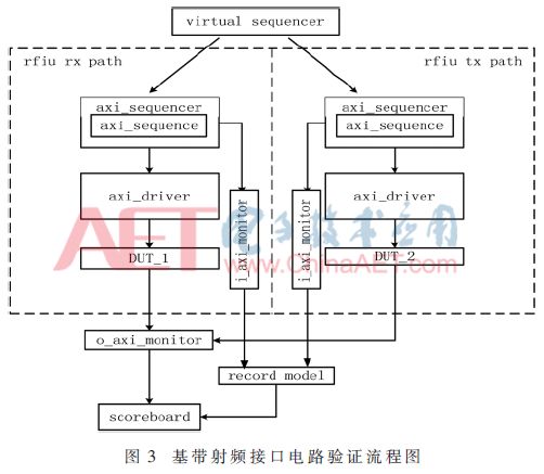
The baseband RF interface uses the AXI bus mechanism to verify the baseband RF receive path module and the transmit path module respectively. The verification process is shown in Figure 3. In the verification environment, the software interface data packet is placed in the virtual sequener, and transmitted to the axi _sequencer through the AXI interface, and the driver obtains the excitation signals generated by the axi_sequence, and the excitation signals respectively act on the verification design of the receiving path and the verification design of the transmission path. Simultaneously, the two axi_monitors not only monitor the data flow of the driver to the RF receiving and transmitting verification design, but also monitor the record model. This record model model realizes the same data transmission function as the RF interface through MATLAB, and puts the data information into the meter. Scoreboard. Another axi_monitor monitors the radio frequency receiving and transmitting path data information transmission to the scoreboard. Once the record model and the monitoring generated data information are transmitted to the scoreboard, the scoreboard will compare the two data to determine whether the simulation is abnormal.
3.2 UVM-based baseband RF interface circuit verification platform
The verification platform of the baseband RF interface circuit is shown in Figure 4. The verification design to be tested is mainly a transmitting module and a receiving module, and the verification object is connected with the verification vector through the interface, and the verification vector is to achieve the same function as the object to be tested. The Agent in the verification environment is provided by the VIP, and the remaining components need to be designed by themselves. The verification environment instantiates two i_axi_agents through the top-level env. These two i_axi_agents contain other verification components, and the internal sequencer, driver, and monitor are created by build_phase, so that each verification component can be tightly connected. The two i_axi_agent component packages are respectively applied to the transmitting module and the receiving module of the radio interface, in order to enable the configured active and passive modes to drive and monitor the data information on the interface. The monitor in the o_axi_agnet instantiation module can monitor the stimulus data stream sent by the test object and send it to the uvm_scoreboard through the TLM interface mechanism. At the same time, the record_model model encapsulated by Matlab monitors the data flow of the transceiver model through the moitor occupied by the passive mode, and monitors the extracted model data stream to be compared with the stimulus data generated by the DUV. The final comparison data flow information is drawn through the uvm_scoreboard scoreboard to determine whether the data information of the baseband RF interface during the transmission and reception process is complete, and whether the statistical coverage requirement is up to standard.
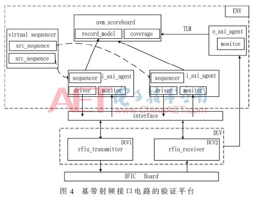
Each register module inside the baseband radio interface transmits the address and data through the APB bus, and the host bridge X2P acts as a general IP to allocate the available address space to the register. These register models can be internally instantiated multiple times, primarily to provide enabling information for the RF transmit and receive paths. The DMA module is used to move the excitation information of the RF transceiver module to the correct memory. Once the limited frame data stream is moved, the interrupt information will be generated. The interrupt information will enter the ARM processor, and the kernel will issue an instruction to block the RF transmission and reception. The introduction of the SPI module enables the RF transceiver to read and write the FIFO normally, while providing mode switching for the external RF daughter board. However, the mode switch inside the baseband RF interface uses the mode register module. These register modules are designed to provide random constraints on the RF transceiver path and to achieve the required stimulus.
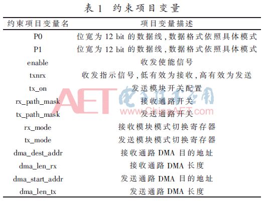
The random constraint information of the RF transceiver path needs to be configured by the software environment of the ARM processor, and the constraint items are stored in the transation data packet, so that the data excitation can become the condition for driving the RF transceiver path, and the RF transceiver module can work normally. At the same time, these constraint items declare the constraint variables, and the variable list is shown in Table 1.
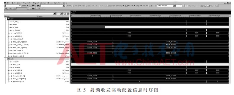
Axi_sequencer transfers the stimulus to the drive axi_driver, which requires software configuration to drive the module under test. The timing diagram for generating RF transceiver driver configuration information is shown in Figure 5. The software configuration environment is as follows: (1) Initialize the RF path, open both the receive and transmit paths, set rx_path_mask to 3 bits, and set tx_path_mask to 15 bits. Mode switching should also be performed here. The software configuration selection interface for rx_mode and tx_mode respectively works in CMOS TDD mode, CMOS FDD mode or LVDS mode. (2) Clock frequency configuration In order to control the external LPCU module to meet the required interface frequency of the corresponding bandwidth. (3) Configure the receive and transmit path enable information, enable to provide the start information of the receive path data source, tx_on provides the location information of the transmit path data source, and txnrx provides the transmit path enable signal for the RFIC simulation model. (4) Input DMA address and DMA length, so that the baseband chip's memory can send or receive data. Once the data stream information is obtained, the interrupt dmareq is issued, and the microprocessor is notified to wait for the next frame data processing, only when the information is enabled. Enable, tx_on, txnrx go low and data transfer ends. (5) Configure the SPI read/write register to control the mode switching of the external RF daughter board, which is consistent with the baseband RF interface mode.
The record model is a model under the MATLAB package. This model includes the transceiver data source module, the data format conversion module, the timing register module, the clock source module, and the transceiver data register module. The data stream of the transceiver data register module is called by the scoreboard. Stored in the FIFO, and then call the comparison function to compare the data stream stored in the FIFO with the data stream in the DUV. If the comparison is consistent, the verification passes; otherwise, the verification fails. The reason for this comparison is that the accuracy of verification is further improved in complex data comparison, and the reference model is rationalized to analyze the completeness and reliability of the function of the RF interface circuit.
3.3 Verification results
This test mainly uses the RFIU TDD 20 M test case as an example to test the function points of the RF transceiver. The function coverage of each function point is counted, and the function coverage of the RF transceiver module is 100%. The RTL of the transceiver path performs code coverage statistics, and the code coverage rate is 100%. Through UVM verification, comparing the data on the scoreboard with the data of the record_model reference model, the role of monitor automatic monitoring is monitored, and the consistency of the data comparison is monitored to be 100%. The functional coverage of the other test cases can reach 100%, and the data comparison degree obtained on the scoreboard is 100%, which can explain that the functional requirements of the RF interface transceiver module have been achieved.
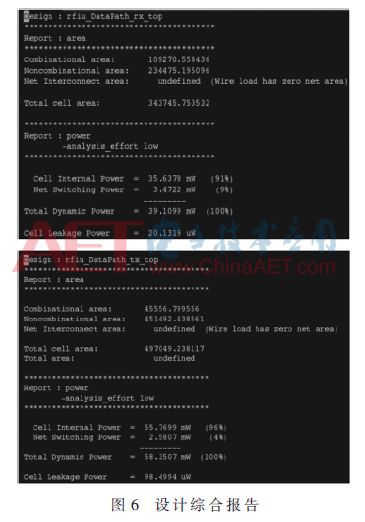
According to Synopsys' Design Compile tool, the RTL code of the RF interface circuit is integrated, and the RF receiving path has a constrained area of ​​0.3 mm2 and a power consumption of 39 mW. The RF interface circuit has a constrained area of ​​0.5 mm2 and a power consumption of 58 mW. . The comprehensive design report is shown in Figure 6.
4 Conclusion
UVM is the cutting-edge methodology for digital IC verification. Although the front-end simulation platform has a long cycle, the execution efficiency is very high, which significantly shortens the verification time of the entire R&D. In this paper, the AXI bus verification component is used to build a UVM-based baseband RF interface circuit verification platform, which realizes the function of the RF interface transceiver module. Within a certain range, the constraint area and power consumption are controlled, which is beneficial to the mass production of the entire baseband chip. At the same time, this verification architecture is used on other modules of the baseband chip, which can improve the verification efficiency and play an important guiding role for the UVM verification platform of the baseband RF interface circuit. It has important application value in digital interface design.
Zhejiang Kaimin Electric Co., Ltd. , https://www.ckmineinverter.com