In order to do a good job of inverter repair, of course, understanding the basic knowledge of the inverter is very important. For the repair of the inverter, it is not enough to understand the above basic circuit. It is also necessary to deeply understand the following main circuits. The main circuit is mainly composed of a rectifier circuit, a current limiting circuit, a filter circuit, a braking circuit, an inverter circuit and a detection sampling circuit. Figure 1 is a structural diagram of it.

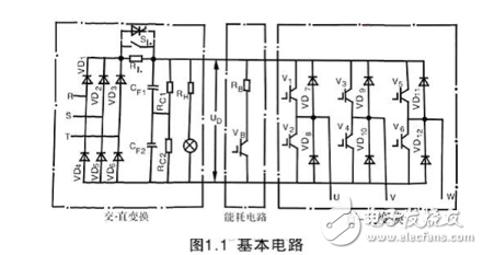
At present, most of the general-purpose inverters are AC-DC-AC inverters, usually the voltage converter is common, and its main circuit diagram (see Figure 1.1) is the core circuit of the inverter. (AC-DC exchange), DC filter circuit (energy-consuming circuit) and inverter circuit (straight-to-transform), of course, including finite current circuit, brake circuit, control circuit and other components.
1) Rectifier circuit
As shown in the figure, the rectifier circuit of the general-purpose inverter is composed of a three-phase bridge rectifier bridge. Its function is to rectify the power frequency power supply, and provide the required DC power supply for the inverter circuit and the control circuit after the intermediate DC link is flattened. The three-phase AC power supply generally needs to be introduced into the input end of the rectifier bridge through the absorption capacitor and the varistor network. The role of the network is to absorb the high-frequency harmonic signals and surge overvoltages of the AC grid, thereby avoiding damage to the inverter. When the power supply voltage is three-phase 380V, the maximum reverse voltage of the rectifier device is generally 1200-1600V, and the maximum rectified current is twice the rated current of the inverter.
2) Filter circuit
The load of the inverter is an inductive load asynchronous motor. Regardless of whether the asynchronous motor is in the electric or power generation state, there is always a reactive power exchange between the DC filter circuit and the asynchronous motor. This non-functional amount depends on the DC intermediate circuit. Energy storage components to buffer. At the same time, the voltage and current output by the three-phase rectifier bridge are DC pulse voltage and current. In order to reduce the fluctuation of the DC voltage and current, the DC filter circuit functions to filter the output of the rectifier circuit.
The large-capacity aluminum electrolytic capacitor of the general-purpose inverter DC filter circuit usually consists of several capacitors connected in series and in parallel to form a capacitor bank to obtain the required withstand voltage value and capacity. In addition, because of the large dispersion of electrolytic capacitor capacity, this will make them unequal in voltage. Therefore, the capacitors must be connected in parallel with a uniform resistance of the resistance phase to eliminate the influence of discreteness, so the life of the capacitor will seriously limit the life of the inverter.
3) Inverter circuit
The function of the inverter circuit is to convert the DC power output from the DC circuit into an AC power source whose frequency and voltage can be arbitrarily adjusted under the action of the control circuit. The output of the inverter circuit is the output of the inverter, so the inverter circuit is one of the core circuits of the inverter and plays a very important role.
The most common inverter circuit structure is a three-phase bridge inverter circuit composed of six power switching devices (GTR, IGBT, GTO, etc.), which regularly controls the turning on and off of the power switching device in the inverter. , can get three-phase AC output of any frequency.
The usual small and medium capacity inverter main circuit devices generally use integrated modules or intelligent modules. The internal height of the intelligent module is integrated with the rectifier module, the inverter module, various sensors, protection circuits and drive circuits. For example, IPMPM50RSA120 produced by Mitsubishi Corporation, 7MBP50RA060 produced by Fujitsu, BSM50GD120 produced by Siemens, etc., internal integration of rectifier module, power factor correction circuit, IGBT inverter module and various detection and protection functions. The module's typical switching frequency is 20KHz, and the protection function is to output fault light when undervoltage, overvoltage and overheat faults.
A freewheeling circuit is provided in the inverter circuit. The function of the freewheeling circuit is that as the frequency decreases, the synchronous speed of the asynchronous motor also decreases. The channel for the regenerative electric energy of the asynchronous motor is fed back to the DC circuit. During the inversion process, the parasitic inductance releases energy to provide a channel. In addition, when two switches located on the same bridge arm are simultaneously turned on, a short circuit occurs and the converter device is burned. Therefore, in the actual general-purpose inverter, various corresponding auxiliary circuits such as a buffer circuit are also provided to ensure the normal operation of the circuit and protect the commutation device in the event of an unexpected situation.
1) Drive circuit
The driving circuit is to provide a driving signal by converting and amplifying the six PWM signals generated by the CPU in the main control circuit as a commutation device (inverter module) of the inverter circuit.
The various requirements for the drive circuit vary with the commutation device. At the same time, some developers have developed a number of dedicated drive modules for various commutation devices. Some brands and models of inverters use dedicated drive modules directly. However, most inverters use drive circuits. From a repair point of view, a more typical drive circuit is introduced here. Figure 2.2 shows the more common driver circuit (see Figure 2.3 for the driver circuit power supply).
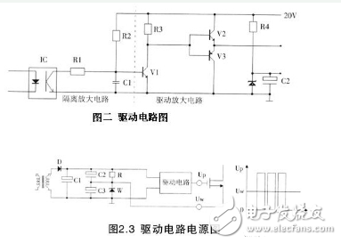
The inverter driving circuit is composed of an isolation amplifying circuit, a driving amplifying circuit and a driving circuit power source. The three upper arm drive circuits are three independent drive power circuits, and the three lower arm drive circuits are a common drive power circuit.
2) Protection circuit
When the inverter is abnormal, the loss caused by the abnormality of the inverter is minimized or even reduced to zero. Each brand of frequency converter pays great attention to the protection function, and tries to increase the protection function and improve the effectiveness of the protection function.
In the field of inverter protection functions, manufacturers can make a good example and make a good article. In this way, the diversity and complexity of the inverter protection circuit are formed. There are regular detection protection circuits and software integrated protection functions. Some inverter drive circuit modules, intelligent power modules, rectifier inverter combination modules, etc., have internal protection functions.
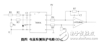
The circuit shown in Figure 2.4 is a typical overcurrent detection protection circuit. It consists of three parts: current sampling, signal isolation amplification, and signal amplification output.
3) Switching power supply circuit
The switching power supply circuit supplies low voltage power to the operation panel, the main control board, the drive circuit, and the fan. Figure 2.5 Structure of the Fuji G11 switching power supply circuit.
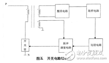
The DC high voltage P terminal is applied to the primary end of the high frequency pulse transformer, and the switch adjusting tube is connected in series with the other primary end of the pulse transformer, and then connected to the DC high voltage N terminal. The switch tube is periodically turned on and off to replace the primary DC voltage with a rectangular wave. The pulse transformer is coupled to the secondary, and after rectifying and filtering, the corresponding DC output voltage is obtained. It compares the output voltage to the pulse width adjustment circuit to change the pulse width to stabilize the output voltage.
4) Communication circuit on the main control board
When the inverter is controlled by a programmable (plc) or host computer, human machine interface, etc., signals must be transmitted to each other through the communication interface. Figure 2.6 shows the communication interface circuit of the LG inverter.
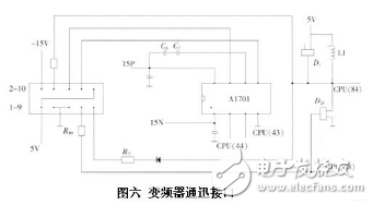
When the inverter communicates, the two-wire RS485 interface is usually used. The same is true for Siemens inverters. The two lines are used to transmit and receive signals, respectively. Before the inverter transmits the signal after receiving the signal, both signals pass through the integrated circuits such as buffers A1701 and 75176B to ensure good communication.
Therefore, the communication interface circuit on the main control board of the inverter mainly refers to this part of the circuit, as well as the anti-interference circuit of the signal.
5) External control circuit
The external control circuit of the inverter mainly refers to the frequency setting voltage input, the frequency setting current input, the forward rotation, the reverse rotation, the jog and the stop operation control, and the multi-speed control. The frequency setting voltage (current) input signal enters the CPU through the A/D conversion circuit in the inverter. Some other controls are passed to the CPU through optocoupler isolation of the input circuitry in the drive.
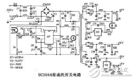
In the following article, upload the maintenance knowledge about the inverter for everyone to share! According to everyone's proposal for me and support for me, I will now contribute some of the most basic and basic knowledge of the inverter. The inverter switching power supply circuit and the inverter switching power supply mainly include an input grid filter, an input rectification filter, a converter, an output rectification filter, a control circuit, and a protection circuit. (http://Copyright) Our company's product switching power supply circuit is shown below. It is a switching circuit composed of UC3844: The switching power supply mainly has the following characteristics: 1. Small size and light weight: Because there is no power frequency frequency converter, the volume and Weight absorption has 20~30% of linear power supply 2, low power consumption and high efficiency: power transistor works in switching state, so the power consumption of transistor is small, conversion efficiency is high, generally 60~70%, and linear power supply is only 30 ~40%
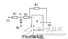
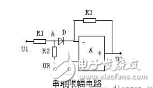
The limiter is an op amp circuit with nonlinear voltage transfer characteristics. The characteristic is that when the input signal voltage is within a certain range, the circuit is in a linear amplification state, and has a constant amplification factor, and beyond this range, enters the nonlinear region, and the amplification factor is close to zero or very low. The requirements in the circuit design of the inverter are also very high. To be a good inverter maintenance technician, it is also very important to understand it.
1. The circuit diagram of the diode parallel limiter is as follows:
2. The diode series limiting circuit is as shown below:
As shown in FIG. 1, the control circuit is composed of the following circuits: an operation circuit for frequency and voltage, a voltage of the main circuit, a current detection circuit, a speed detection circuit for the motor, a drive circuit for amplifying the control signal of the operation circuit, and an inverter. Protection circuit for the motor and the motor.
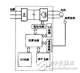
In the dotted line of Fig. 1, the speedless detection circuit is open loop control. The speed detection circuit is added to the control circuit, that is, the speed command is increased, and the speed of the asynchronous motor can be controlled to more precisely closed-loop control.
1) The arithmetic circuit compares the external speed and torque commands with the current and voltage signals of the detection circuit to determine the output voltage and frequency of the inverter.
2) The voltage and current detection circuit is isolated from the main circuit potential to detect voltage and current.
3) Drive circuit
To drive the circuit of the main circuit device, it is isolated from the control circuit to turn the main circuit device on and off.
4) I/0 input and output circuit
In order to better human-machine interaction of the inverter, the inverter has a variety of input signal input (such as running, multi-speed operation, etc.) signals, as well as various internal parameters of the output "such as current, frequency, protection action drive, etc." signals.
5) Speed ​​detection circuit
The signal of the speed detector (TG, PLG, etc.) mounted on the asynchronous motorized shaft machine is sent to the arithmetic circuit as a speed signal, and the motor can be operated at the command speed according to the command and calculation.
6 ) Protection circuit
Detect the voltage, current, etc. of the main circuit. When an abnormality such as overload or overvoltage occurs, prevent the inverter and the asynchronous motor from being damaged, stop the inverter or suppress the voltage and current values.
The protection circuit in the inverter control circuit can be divided into two types: inverter protection and asynchronous motor protection. The protection functions are as follows:
HCPL-316J characteristics of inverter drive circuitHCPL-316J is an IGBT gate drive optocoupler manufactured by Agilent. It integrates the collector emitter voltage undersaturation detection circuit and fault state feedback circuit to ensure the reliable operation of the drive circuit. Its characteristics are: compatible with CMOS / TYL level; optical isolation, fault state feedback; switching time up to 500ns; "soft" IGBT off; under saturation detection and undervoltage lockout protection; overcurrent protection; wide operating voltage range (15 ~30V); user can configure automatic reset, automatic shutdown. The DSP and the coupler combine to realize the driving of the IGBT, so that the IGBT VCE undersaturation detection structure is compact, low-cost and easy to implement, and meets a wide range of safety and regulation needs.
Implementation of HCPL-316J protection function
HCPL-316J has built-in rich IGBT detection and protection functions, making the drive circuit more convenient, safe and reliable. The following sections describe how the undervoltage lockout protection (UVLO) and overcurrent protection functions:
(1) IGBT undervoltage lockout protection (UVLO) function
During the power-on process, the chip supply voltage gradually rises from 0V to the maximum value. If the chip has an output that causes the IGBT gate voltage to be too low, it will operate in the linear amplification region. The undervoltage lockout protection (UVLO) of the HCPL316J chip solves this problem. When the voltage between VCC and VE is less than 12V, the low level is output to prevent the IGBT from operating in the linear working area and causing excessive heat and burning. The schematic is shown in Figure 1 with the UVLO section.
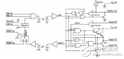
Figure 1 HCPL-316J internal schematic
(2) IGBT overcurrent protection function
The HCPL-316J has an overcurrent protection function for the IGBT, which performs protection by detecting the on-voltage drop of the IGBT. It can also be seen from the figure that there is a fixed 7V level inside it. When the detection circuit is working, it will detect the voltage drop across the C-E pole of the IGBT compared with the built-in 7V level. When it exceeds 7V. The HCPL-316J chip outputs a low level to turn off the IGBT. At the same time, an error detection signal is fed back to the input side through the on-chip optocoupler, so as to take corresponding solutions. When the IGBT is turned off, the voltage across the C to E poles must exceed 7V, but at this time, the overcurrent detection circuit fails, and the HCPL-316J chip does not report the fault signal. (http://Copyright) In fact, due to the tube voltage drop of the diode, the chip takes protection action when the voltage between the C and E poles of the IGBT is less than 7V.
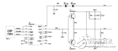
The entire board acts as an optocoupler isolation amplifier. The core part is the chip HCPL-316J, in which the controller (DSP-TMS320F2812) generates XPWM1 and XCLEAR* signals to the HCPL-316J, and the HCPL-316J generates the IGBT fault signal FAULT* to the controller. At the same time, a push-pull output circuit composed of NPN and PNP is connected to the output end of the chip, in order to improve the output current capability and match the IGBT drive requirements.
When the output of the HCPL-316J output is high, the upper tube (T1) of the push-pull circuit is turned on, the lower tube (T2) is turned off, and the output of the three-terminal regulator LM7915 is applied to the IGBT gate (VG1). The VCE is 15V and the IGBT is turned on. When the output of the HCPL-316J output VOUT is low, the upper tube (T1) is turned off, the lower tube (T1) is turned on, VCE is -9V, and the IGBT is turned off. The above is the turn-on and turn-off process of the IGBT.
Data Acquisition Adcs Dacs,Ics Data Acquisition Adcs/Dacs,Data Acquisition Adc / Dac Professional,Ic Chip Data Acquisition Adcs/Dacs
Shenzhen Kaixuanye Technology Co., Ltd. , https://www.icoilne.com