With the rapid development of image processing, industrial control, wireless communication and other fields, the performance requirements of data acquisition systems such as speed and accuracy are also increasing. These requirements pose new challenges to the design and implementation of data acquisition systems. The current design of data acquisition systems is usually divided into the following categories:
1) Based on the single control chip and A/D converter of the microprocessor, the design scheme is simple, and in the application where the performance is not high, in order to reduce the cost, a microprocessor integrated with the A/D converter can be used.
2) Using a general-purpose computer to configure the data acquisition card, it is usually necessary to develop a computer-side application that can perform complex calculations, but the corresponding drivers of different capture cards are different. If the demand changes, the corresponding application needs to be replaced. It also needs to be redeveloped. Therefore, the design scheme has poor versatility and low real-time performance.
3) ARM and FPGA or DSP and FPGA combination as the core of the acquisition system, ARM processor is suitable for control field, DSP processor is suitable for signal processing field, FPGA device is suitable for high-speed parallel acquisition and processing field due to its own characteristics, with ARM Or DSP and other processors can not match the advantages. This type of combination combines the characteristics of each, with strong processing capabilities and a wide range of applications.
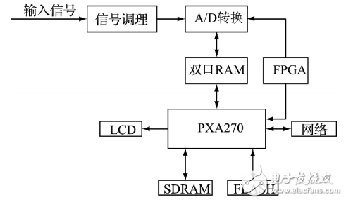
Data exchange between ARM and FPGA uses a dual-port RAM chip to implement FIFO functions. The ARM processor in the system acts as the system control core, and is responsible for controlling the working sequence of the entire system and uploading the data to the server for storage through the network. The FPGA is responsible for mode configuration and data transmission of the A/D converter. This combination method combines the advantages of ARM in control and FPGA in acquisition, and has the characteristics of strong versatility and flexible configuration.
2, system designThe system hardware is mainly composed of signal conditioning circuit, analog-to-digital converter ADS1278, FPGA device CyCLOnE series EP1C6, dual-port RAMIDT7205 and processor PXA270 and peripheral circuits. The system structure block diagram is shown in Figure 1. After the input signal passes through the signal conditioning circuit, it enters the A/D converter for data conversion, converts the analog signal into 23-bit mantissa and one-sign bit data, and the FPGA configures the A/D converter and stores the converted data in order. In the port RAM, when the conversion data storage is full, the ARM processor is interrupted, and the ARM processor reads the data from the dual port RAM for calculation, and transmits the collected data to the server through the network interface.

Figure 1 System structure
2.1, 24-bit A/D conversion chip ADS1278The ADS1278 is a 24-bit 8-channel simultaneous sampling sigma-delta ADC with a sampling rate of up to 128 KS/s from Texas Instruments. Support multiple operating modes, internal integrated linear phase digital filter, data output interface supports SPI or optional frame synchronization, easy to interconnect with FPGA. It can meet defense, aerospace and medical applications.
The digital filter integrated in the ADS1278 converter extracts the input signal into a 1-bit high-resolution digital signal by Nyquist sampling. The 8-channel input signals enter separate 8 A/D converters, which are internally composed of high-order choppers, digital filters, and modulators. The input analog signals can be passed through high-order filters to obtain digital signals. Figure 2 shows the clock and data timing diagram for the ADS1278 in SPI format.

Figure 2 Timing in SPI format
Copper Tube Terminals Without Checking Hole
Our company specializes in the production and sales of all kinds of terminals, copper terminals, nose wire ears, cold pressed terminals, copper joints, but also according to customer requirements for customization and production, our raw materials are produced and sold by ourselves, we have their own raw materials processing plant, high purity T2 copper, quality and quantity, come to me to order it!
Copper Tube Terminals Without Checking Hole,Cable Lugs Insulating Crimp Terminal,Cable Connector Tinned Copper Ring Terminal,Tubular Cable Lugs Crimp Terminal
Taixing Longyi Terminals Co.,Ltd. , https://www.longyicopperterminals.com