Micro LED technology has been fired and shocked, it is the dominant display technology of the next generation, and it is the star of display in 2018. However, there are still many problems in the current Micro LED. Whether it is process technology, inspection standards, or production cost, it is far from a large number of commercial applications. One of the most important challenges is how to import mass production. Reduce its manufacturing costs, and this link is called "huge transfer."
To understand the huge amount of transfer, of course, you must first know what a Micro LED is and how it differs from a traditional LED. The full name of the Micro LED is "Micro Light Emitting Diode", which is also called micro-light-emitting diode in Chinese. It can also be written as "μLED".
The biggest difference from the general LED is of course the size. However, the size is called Micro LED, and there is still no uniform standard, so it is the case of the manufacturer. Taking the definition of Taiwanese wafers as an example, the general LED die is between 200 and 300 micrometers (micrometer, μm), and the Mini LED (called Micro LED precursor) is about 50 to 60 micrometers, while the micro LED is 15 microns.
μLED wins all display technologies, cost and mass production are the only challenges
Due to the difference in grain size, their respective applications are different. The general LED chip is mainly for lighting and display backlight module; as for the Mini LED, it will also be used in backlight applications, but it will be in high-end consumer products, or in the automotive market, such as Innolux's AM miniLED. Used in the car display; as for the Micro LED, its application concept is completely different from the former two, it will be a new display technology, and its competitor will be OLED.
From the technical specifications and application concepts, μLED is superior to the current display technology in terms of brightness, response speed, power consumption and durability. It can almost be said to have the potential to completely replace LCD and OLED displays, but the only problem is Its production cost and capacity for mass production.

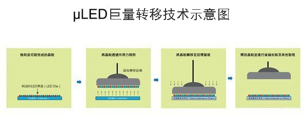
At present, the biggest production challenge of μLED is how to place a huge amount of micron-sized LED chips on a target substrate or circuit through a high-precision device, and this program is called a massive transfer (Mass). Transfer).
In fact, massive transfer is an academic term that is often used in the engineering of material handling processes involving the diffusion and convection of matter or particles within a physical system.
More specifically, massive transfer is a description of a chemical or physical mechanism. It is a transport phenomenon that means that a large number of points (molecules or particles) move from one end to the other. It can be a single stage, or multiple stages, and involves a liquid or gas phase, sometimes in solid matter.
A classic example of massive transfer is the “evaporation†of water. Through evaporation, a large amount of water particles can be moved to another substance. Similarly, diffusion is also true.
How to handle the challenges of tens of millions of micron-sized LED dies
For the production of μLED, it is necessary to correctly and efficiently move millions or even tens of millions of micron-sized LED chips onto a circuit board. Taking a 4K TV as an example, the number of crystals that need to be transferred is as high as 24 million (calculated in three colors of 4000 x 2000 x RGB), and even if it is transferred 10,000 times, it needs to be repeated 2,400 times.
The Taiwan Institute of Technology is also currently working on the development of a large number of related technologies, and the main responsible unit is the Institute of Electronics and Optoelectronic Systems. Dr. Wu Zhiyi, director of the Electro-Optical Institute, said: "The current LED and display panel process is relatively mature. The biggest difficulty is how to transfer such a large number of μLED dies."
Dr. Wu Zhiyi pointed out that although it is not easy to produce micron-sized μLED crystal grains, there are still equipments that can be done, but the yield and yield problems. For example, the red LED shrinks to the micron level, there is a problem that the silicon material is fragile, but there are still some problems. The law is feasible, and there is still no good solution for the huge transfer.
Because of the high technical difficulty of the yield and efficiency of huge transfers, Apple, Samsung and Sony are actively researching breakthroughs.
Dr. Wu Zhiyi said that the principle of achieving a huge amount of transfer is actually very simple, that is, to generate a force to accurately adsorb the μLED die, and then transfer it to the target back plate, and then release it accurately. The principles that can be used are: vacuum, static electricity, adhesion, UV and electron effects.
The key question is how much yield can be achieved and whether capacity is cost effective.
If you don't consider the production capacity, you can also make a μLED display panel through the current transfer equipment, such as Pick-and-Place, but the cost will be very expensive, unless it is very insensitive to customers and applications. It is difficult to have room for business development.
Several companies have announced their initial success on small-size panels, including PlayNitride in Taiwan, Crystal, LuxVue acquired by Apple, Sony in Japan, and Samsung in South Korea, but these companies They did not disclose the form and technology of their transfer. Of course, production and production capacity were not announced.
At this year's CES 2018 show, Samsung showed the 146-inch Micro LED TV "The Wall", which uses modular splicing to achieve a large-sized panel effect.
Compared with μLED, which urgently needs huge transfer technology to solve the problem of mass production, Mini LEDs with grain sizes between 50 and 60 microns can be mass-produced using existing production equipment. Therefore, current LED manufacturers are all First choose the products to be put into this transition, and even the Micro LED products previously released by Samsung and Sony may be products that belong to the Mini LED grade and are produced through existing equipment.
The frequent actions of these international giants have certainly attracted the attention of the market. However, in the research and development of μLED technology, China and Taiwan are not backward, and may even have opportunities ahead. The Taiwan Institute of Technology began investing in the development of μLED technology as early as 2009, but it did not have to go to the mainstream display application development at the beginning, but with the evolution of the market and technology, it gradually realized the potential of its market.
"At the time, we thought that OLEDs could be, and LEDs would certainly be able to do it," said Dr. Wu Zhiyi.
He pointed out that in theory, LED can replace all current OLED display products. The only problem is the manufacturing cost and the so-called C/P value. If the price of the product is high and there is no interest, then there is no development. value. This is almost the case with OLED TVs a few years ago.
For the huge amount of transfer technology, Dr. Wu Zhiyi revealed that the Taigong Institute has already had relevant solutions, but he still can't disclose relevant information. He only responds to the relevant technology announcements this year. Please wait and see.
However, he believes that the most feasible process for mass transfer is still on 6å‹ to 8å‹ wafers, and it is mainly used for small-sized display applications. Large-size display applications can only be carried out through collage. Solve the problem of production costs; as for the technical form of use, it will be transferred by means of adsorption, that is, using static electricity, van der Waals or other forces.
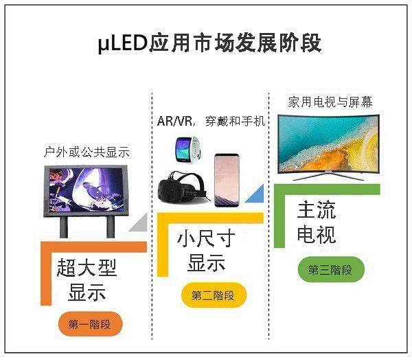
μLED application market will show M-type development
Because the transfer technology is not easy, and the output and yield are limited, the application market of μLED will be developed by M-type, that is, starting from the two sizes of maximal and minimum, and finally gradually increasing the quantity. The largest consumer electronics and TV sizes are coming up. But whether it can develop into the mainstream consumer electronics market, or even replace the current OLED TV or LCD TV, it will depend on the production cost at that time.

Dr. Wu Zhiyi said that because the characteristics of LEDs are that the light-emitting area is smaller than the component area, it is very suitable for splicing to produce oversized display panels, especially large-sized displays for outdoor or public spaces, plus these applications for price. The sensitivity is not high, so it will be the first commercial market for μLED display.
And after the oversized size, it will be ultra-small display applications, such as wearable and AR / VR devices, especially AR and VR. Dr. Wu Zhiyi said that the high brightness, low power consumption and high response speed of μLED are very suitable for these applications. They can not only overcome the problems displayed in daylight, but also improve power consumption, and also meet the high-speed display requirements of games.
However, Dr. Wu Zhiyi does not believe that μLED will enter the consumer electronics market in large numbers, especially in the general home TV market. He believes that the current production cost of μLED is still very expensive. Even if the process is mature, it will be much higher than LCD panels. Even if the display performance is excellent, it is not easy to convince consumers to buy, so it will take some time to observe.
But at least it is clear that one thing is that before the huge transfer technology matures, the products and applications of μLED are far away from the actual commercial market, and the most specific technology will be available until the second half of this year. The details are revealed. Until then, all about μLED, I am afraid it is just a vision and topic.

Modular Plug,modular jack rj45,modular jack cat6,mod plugs
NINGBO UONICORE ELECTRONICS CO., LTD , https://www.uonicore.com