One of the advantages of LLC is that it can realize the zero voltage turn-on (ZVS) of the primary side MOSFET within a relatively wide load range, and the turn-on loss of the MOSFET is theoretically reduced to zero. To ensure the ZVS of the LLC primary side MOSFET, the following three basic conditions need to be met:
1) 50% duty cycle of upper and lower switching tubes, 1800 symmetrical driving voltage waveform;
2) Inductive resonant cavity and sufficient inductive current;
3) There must be enough dead time to maintain ZVS.
[LLC crowdfunding] The most complete Zhang Fei half-bridge LLC resonant switching power supply tutorial in history! Crowdfunding last 6 days>Click here to participate immediately
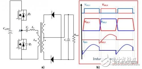
Figure a) is a typical LLC series resonant circuit. Figure b) is the operating waveform of the MOSFET under inductive load. Because under the inductive load, the current phase will lead the voltage, so the ZVS of the MOSFET operation is guaranteed. To ensure that the MOSFET runs in the inductive region, the resonant current on the resonant inductor must be large enough to ensure that the charge stored on the equivalent parasitic capacitance between the source and drain of the MOSFET can be completely released during the dead time.
When the MOSFETs on the primary side are all in the off state, the resonant current in the series resonant circuit will charge and discharge the equivalent output capacitance of the switching MOSFET. The equivalent circuit when all MOSFETs are turned off is shown in the figure below:
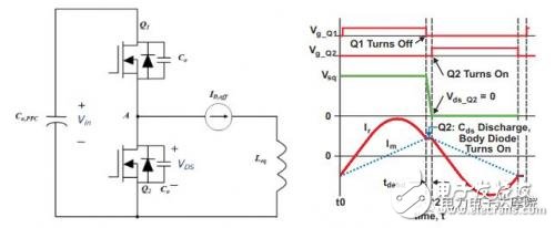
Through the analysis of the above figure, it can be concluded that the two necessary conditions for ZVS need to be met, as follows:

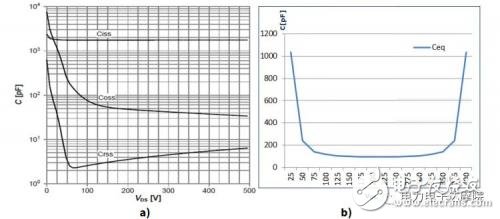
Although the formula looks simple, a practical situation about the equivalent output capacitance of the MOSFET Ceq is that the equivalent parasitic capacitance of the MOSFET is a function of the source-drain voltage Vds. The previous article gave a detailed theory of the equivalent parasitic capacitance of the MOSFET. And actual introduction. In other words, the equivalent capacitance value will change with the change of Vds. As shown in the figure below, take Infineon's IPP60R190P6 as an example:
The Vds discharge process of the LLC series resonant circuit MOSFET is divided into four stages, as shown in the following figure, (I) 380V-300V; (II) 300V-200V; (III) 200V-100V; (IV) 100V-0V.
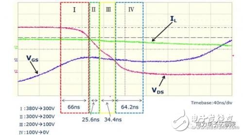
It can be seen from the figure that the two parts (I) and (IV) occupy nearly 2/3 of the Vds discharge time. At this time, the inductor current of the resonant cavity is basically unchanged. The main reason why these two parts occupy most of the time of Vds discharge is that when Vds drops to close to 0, the parasitic capacitance Coss between the source and drain of the MOFET will increase exponentially. Therefore, to completely release this part of the charge, a longer LLC resonance period and release time are required.
Therefore, choosing a suitable MOSFET (sufficiently small equivalent parasitic capacitance) is essential for the realization of ZVS, especially when Vds is close to 0, the equivalent output capacitance should be small enough, which can further reduce the dead time and Improve the work efficiency of LLC.
The figure below further illustrates how to choose a suitable ZVS solution.
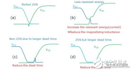
Figure (a): Ideal ZVS waveform;
Figure (b): Vds has not dropped to 0, Vgs has appeared. In this case, the LLC series resonance will have hard switching. The countermeasures need to reduce the excitation current of the transformer, or increase the dead time appropriately (if the IC is selected, the dead time is generally fixed);
Figure (c): ZVS is achieved, but the current in the resonant cavity is not enough to maintain the continuous conduction of the diode in the MOSFET.
Figure (d) The dead time is too long, which will reduce the efficiency of the entire LLC.
In short, the equivalent output capacitance of the MOSFET is crucial to the realization of the LLC primary MOSFET ZVS. If the MOSFET has been selected, the resonant cavity needs to be carefully calculated, adjusted and set, and an appropriate dead time is selected to cover the application range of all loads. In practical applications, the hard switches of steady-state operation can be modified by design to achieve the design goal of stable operation. However, hard switching during the boot process (from soft start to high frequency to low frequency), especially the first few switching cycles during the boot process, is unavoidable for some designs and solutions.
Capacitive Touch Membrane Switch
Capacitive touch screen technology uses the human body's current induction to work. The capacitive touch screen is a four-layer composite glass screen. The inner surface of the glass screen and the interlayer are coated with one layer of ITO, and the outermost layer is a thin silica glass protective layer. The interlayer ITO coating is used as the working surface, and four electrodes are drawn from the four corners, while the inner ITO is the shielding layer to ensure a good working environment. When the finger touches the metal layer, a coupling capacitor is formed between the user and the touch screen surface due to the human electric field. For high frequency current, the capacitor is a direct conductor, so the finger draws a small current from the contact point. The current flows from the electrodes at the four corners of the touch screen respectively, and the current flowing through the four electrodes is proportional to the distance between the finger and the four corners. The controller obtains the position of the touch point through the accurate calculation of the ratio of the four currents.
China Membrane Switch,Membrane Switch Manufacturer,Membrane Switch
KEDA MEMBRANE TECHNOLOGY CO., LTD , https://www.kedamembrane.com