The SRAM can store its internal stored data without requiring a refresh circuit. The DRAM (Dynamic Random Access Memory) is refreshed and charged once every other time, otherwise the internal data will disappear, so the SRAM has higher performance, but the SRAM also has its disadvantages, namely its low integration, the same The capacity of the DRAM memory can be designed to be a small size, but the SRAM needs a large volume and consumes a lot of power. So on the motherboard SRAM memory takes up a part of the area.
Main specificationsOne is a cache between the CPU and the main memory. There are two types of memory: one is the cache memory (Cache Memory) fixed on the motherboard; the other is the COAST (Cache On A) inserted in the card slot. STIck) is used for the expansion of the cache. In addition, in the circuit of the CMOS chip 1468L8, it also has a small capacity of 128 bytes of SRAM, which stores the configuration data we set. In order to speed up the transfer of CPU internal data, since the 80486CPU, the internal cache is also designed in the CPU, so the PenTIum CPU has the so-called L1 Cache (L1 cache) and L2Cache (L2 cache) Generally, L1 Cache is built into the CPU. L2 Cache is designed outside the CPU. However, PenTIum Pro designs L1 and L2 Cache at the same time inside the CPU, so the volume of PenTIum Pro is large. The latest Pentium II moves L2 Cache to a black box outside the CPU core. SRAM is obviously fast and does not require refresh operation, but it also has other shortcomings: it is expensive and bulky, so it cannot be used as a main memory on the main board.
Basic FeaturesIts characteristics are summarized as follows:
â—ŽAdvantages, speed, do not have to match the memory refresh circuit, can improve the overall work efficiency.
â—Ž Disadvantages, low integration, large power consumption, large volume of the same capacity, high price, and a small amount for critical systems to improve efficiency.
â—Ž System used by SRAM:
â—‹ Cache between CPU and main memory.
â—‹ Internal L1/L2 or external L2 cache in the CPU.
â—‹ COAST cache for CPU external expansion.
â—‹ CMOS 146818 chip (RT & CMOS SRAM).
The main purposeSRAM is mainly used for Level 2 cache. It uses transistors to store data. Compared with DRAM, SRAM is fast, but the capacity of SRAM in the same area is smaller than other types of memory.

SRAM SRAMs are fast but expensive, and generally use small-capacity SRAMs as caches between higher-speed CPUs and lower-speed DRAMs. There are also many kinds of SRAMs, such as AsyncSRAM (Asynchronous SRAM) and Sync SRAM (Synchronous SRAM). , Synchronous SRAM), PBSRAM (Pipelined Burst SRAM, Streaming Burst SRAM), and CSRAM with tel/'target='_blank'> INTEL not announced details.
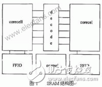
The basic SRAM architecture is shown in Figure 1. SRAM can be divided into five major parts: memory cell array, row/column address decoder, Sense Amplifier, and control circuit (control). Circuit), Buffer/Driver Circuit (FFIO). SRAM is a static storage mode. A bistable circuit is used as a memory cell. SRAM does not need to be constantly refreshed like DRAM, and its working speed is fast. However, due to the large number of memory cell devices, the integration is not very high and the power consumption is also large.
working principle
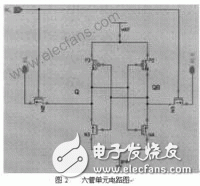
Figure 2 The working principle of the six-cell circuit SRAM:
Suppose that a “1†is to be written to the 6T memory cell in FIG. 2 , first a group of address values ​​are input to the row and column decoders, a specific cell is selected, and then the write enable signal WE is valid and will be written. Data “1†is written to the two bit lines BL, BLB of the selected cell after the write circuit becomes “1†and “0†respectively. At this time, WL=1 of the selected cell, the transistors N0, N5 are turned on, and BL is turned on. The signals on the BLB are sent to the Q and QB points respectively so that Q=1 and QB=0, so that the data “1†is latched in the latch formed by the transistors P2, P3, N3, and N4. The process of writing data "0" is similar.
The read process of SRAM reads “1†as an example. The bit line BL/BLB is pre-charged to the power supply voltage VDD by the decoder selecting a certain bit line. After the precharge is completed, a row is selected by the row decoder. A memory cell is selected, because it is stored in the "1", then WL = 1, Q = 1, QB = 0. Transistors N4 and N5 are turned on, and current flows through N4 and N5 to ground, so that the potential of BLB decreases, and the voltage difference between BL and BLB generates a voltage difference. When the voltage difference reaches a certain value, the sensitivity amplifier is turned on, the voltage is amplified, and then sent to the output. Circuit, read data.
Structure principleSRAM (Static RAM), which is static RAM. It is also composed of transistors. Turn on the representative 1 and turn off the indication 0, and the state will remain until a change signal is received. These transistors do not need to be refreshed, but they will lose information when they are shut down or powered down. SRAM is very fast and usually works at 20ns or faster. A DRAM memory cell requires only one transistor and one small capacitor. Each SRAM cell requires four to six transistors and other parts. Therefore, in addition to being more expensive, the SRAM chip is also larger in appearance and takes up more space than DRAM. SRAM and DRAM are not interchangeable because of the difference in appearance and electrical.
The high speed and static nature of SRAMs makes them often used as cache memory. The computer's motherboard has a Cache socket.

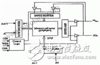
SRAM The following figure shows the block diagram of an SRAM. From the above figure, it can be seen that the SRAM is generally composed of five major components, namely, a memory cell array, an address decoder (including a row decoder and a column decoder), a sensitive flamer, a control circuit, and a buffer/driver circuit. In the figure, A0-Am-1 is the address input terminal, and CSB. WEB and OEB are the control terminals. They control read and write operations and are active low, and 1100-11ON-1 are data input/output terminals. Each memory cell in the memory array shares electrical connections with other cells in rows and columns. The horizontal wire is called "word line", and the vertical data flow into and out of the memory cell is called " Bit line." A specific word line and bit line can be selected by the input address. The intersection of the word line and the bit line is the selected memory cell. Each memory cell is uniquely selected in this way and then read and written. operating. Some memories are designed for multi-bit data such as 4-bit or 8-bit simultaneous input and output. In this case, four or eight memory cells will be selected for read and write operations in the same manner as above.
In the SRAM, arrays of memory cells arranged in a matrix form are decoders and interface circuits with external signals. Memory cell arrays are usually in the form of squares or matrices to reduce the overall chip area and facilitate data access. Taking an SRAM with a storage capacity of 4K bits as an example, a total of 12 address lines are required to ensure that each storage unit can be selected (212=-4096). If the memory cell array is arranged to have only one column of bars, a 12/4K bit decoder is required, but if it is arranged to contain 64 rows and 64 columns, only one 6/64 bit is needed. The row decoder and a 6/64-bit column decoder, row and column decoders can be arranged on both sides of the memory cell array, 64 rows and 64 columns have a total of 4096 intersections, each corresponding to a point Storage bit. Therefore, arranging the memory cells in a square shape rather than in a long row in a row greatly reduces the entire chip area. In addition to the shape singularity and large area, the memory cell array has a disadvantage in that the line connecting the memory cell and the data input/output terminal in the upper part of the column becomes very long, especially for a relatively large capacity. In memory, the situation is more serious, and the delay of the connection is at least linear with the length of the connection. The longer the connection, the greater the delay on the line, so it will lead to a reduction in the read and write speed and different The inconsistencies in the connection delays of the memory cells are all required in the design.
Stereo headphone is important components of audio equipment. It has a wide frequency response, low distortion, power saving, strong audio resolution, clear surround sound, and good music rhythm. Stereo headphone is divided into earphone and headphone, which has the difference of left and right channels. It cannot be used interchangeably. Otherwise, the fidelity of the sound source and the resolution of the source frequency will be directly affected.

Stereo Headphones,Wireless Stereo Headphones,Bluetooth Stereo Headphones,Wireless Bluetooth Stereo Headphones
Shenzhen Linx Technology Co., Ltd. , https://www.linxheadphone.com