It is proposed that due to the increase of FPGA capacity and the lengthening of configuration time, the conventional design will lead to the failure of system function. By describing in detail the various configuration methods of Xilinx FPGA and its advantages and disadvantages in circuit design, the configuration steps and working timings of FPGA power-on and the I/O pin status of each stage are analyzed in depth, and the FPGA power-on configuration circuit is explained. The serious impact of the function, and finally put forward effective design recommendations for FPGA peripheral circuits with different functional requirements.
1 IntroductionWith the rapid development of semiconductor and chip technology, today's FPGAs integrate more and more configurable logic resources, a variety of external bus interfaces and a wealth of internal RAM resources for defense, medical, consumer electronics, etc. The field has become more and more widely used. However, most FPGAs are based on SRAM technology and are volatile. Therefore, FPGAs usually use external storage devices (such as PROM) to store the necessary configuration information to prevent the FPGA from losing self-configuration capability after the device is powered down. However, the FPGA configuration can be successfully completed under certain conditions and time. As the capacity of the FPGA continues to rise, the configuration time is greatly lengthened. If the FPGA is not fully considered, the configuration timing of the FPGA and the impact on other devices are based on conventional experience. Designing a circuit often affects the normal operation of other peripheral devices of the system, and in severe cases, the entire system fails. Therefore, FPGA configuration and power-up timing have become an important part of system design.
2 Xilinx FPGA configuration and featuresXilinx FPGA supports a variety of configuration methods, including Serial Master Mode (Slave Serial), Serial Slave Mode (Master SelectMAP), Parallel 8-Bit Slave Mode (Slave Select MAP8), Parallel 32-bit Slave Select MAP32, as well as Boundary Scan Mode (JTAG), adds support for SPI and BPI interface Flash after the Virtex5 device.
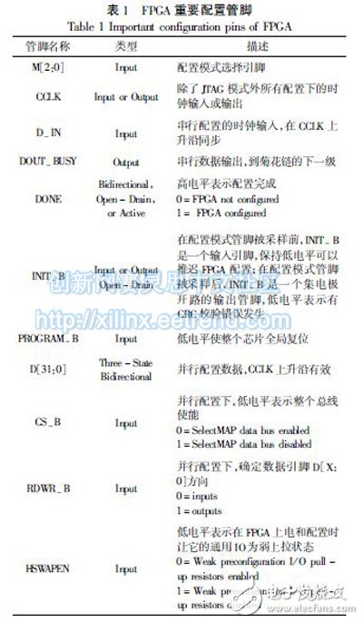
In the current design, the serial master mode and the parallel master mode are commonly used. The common feature is that the circuit hardware design does not need to be connected to a configuration clock, and the FPGA itself provides the clock during configuration, thus reducing The difficulty of PCB design and the timing interference caused by the clock. But they also have their own advantages and disadvantages. The circuit design of the parallel configuration is relatively complicated, and some versatile configuration pins are needed. If the impedance matching and the equal length of the data lines are also considered in the complicated or high-speed configuration circuit, the PCB design difficulty is increased. Therefore, when selecting the FPGA configuration mode, it is necessary to select the correct configuration according to the power-on initialization time of the peripheral device, the degree of influence affected by the FPGA configuration, and the complex characteristics of the circuit. At the same time, the necessary configuration pins need to be processed accordingly, and detailed analysis will be performed later. Table 1 shows the important configuration pins and definitions for the FPGA. As you can see, some configuration pins are only needed in parallel mode.

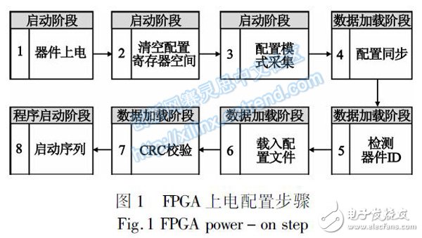
FPGA and CPLD are different, power-on can not work directly, it requires a configuration process. Xilinx FPGA needs 8 steps to run normal running user logic. The whole process is shown in Figure 1.

3.1 FPGA power-on startup
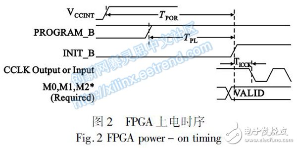
The first step in FPGA operation is to power up the device. Xilinx requires VCCINT (core voltage) to move first, then VCCO (I/O voltage), and the worst case is that they can't differ by more than 1 s. In parallel configuration mode, VCCO_2 requires the same reference voltage as the PROM reference voltage. The power-on process is shown in Figure 2. Among them, TPOR (Power-on-Reset) is 5~30ms, T(PL)(Program Latency) is Max 4ms, T(icck)(CCLK(output delay) is Min500ns.

When the system is powered up normally or PROG-B is a low pulse, the FPGA begins to configure the register space. During this time, except for the defined configuration pins, other I/O pins are set to high-Z (High-Z). After many tests, this phase takes about 30ms.
The final step in the FPGA startup phase is to configure the boot mode. As PROG-B goes high, the FPGA begins to acquire the configuration mode pins (M3, M2, M1) and simultaneously drives the CCLK output. At this stage, there are two ways to delay the configuration timing of the FPGA. One is to pull down the INIT-B pin. This is because the FPGA has detected that it has not been initialized yet and will not proceed to the next step until INIT- The B pin becomes high. The other is to pull the PROG-B pin low so that the FPGA is still waiting for configuration.
3.2 FPGA data loading
Before the normal data loading of the FPGA, a synchronization check between the device and the PROM is required. The method is to transfer a special 32-bit value (0xAA995566) to the FPGA, prompting the FPGA to start transmitting the configuration data. This step is transparent to the user because it is generated in the Xilinx ISE Bitstream Generator. This check code has been automatically added to the bit file.
After the communication synchronization before the configuration is completed, the FPGA and the PROM cannot identify each other, so Xilinx designs a unique device ID number for each model of the FPGA. This ID number can be found in the Xilinx Configuration Manual. Found in the middle. The XC4VS35 used in the above example has an ID number of 0x02088093. The FPGA needs to read the device number and its own comparison from the PROM. If it is the same, continue with the following steps. If not, the configuration fails and the configuration fault information is printed out.
After all the preparations are completed, the FPGA starts loading the configuration file. This step is also transparent to most users and is done by the device itself. This is also the most time consuming step in the configuration process, ranging from 100ms to a few seconds. During this process, all configurable I/O of the FPGA becomes weak pull-up (HSWAPE=1) or high-impedance state (HSWAPE=0) according to the setting of the HSWAPEN pin. The I/O pins at this stage have not yet become the state that the user needs, and are most likely to affect the power-up timing and operation of other peripheral circuits. Pay special attention to and take necessary measures when designing the hardware circuit, such as adding the pull-up resistor, changing the power-on sequence of the device, etc. to avoid or reduce the influence of the FPGA configuration on other devices of the circuit.
After the configuration file is loaded, in order to verify the correctness of the data, the FPGA also automatically sets the CRC check (this can also be removed in the ISE configuration options, but this must be selected to ensure the correctness of the loaded data). If the CRC check is not correct, the FPGA will automatically pull INIT-B low, giving up this configuration. The user must pull the PROG-B pin low to reconfigure.
CAT5E Keystone Jack is an integral parts of RJ45 networking connectors for speed voice, video, data server center, CAT5E keystone jacks are an integral part of any high speed voice, data, or video network. These standardized female connectors are used for inserting multi-conductor Ethernet cable into wall plates, patch panels, or surface mount boxes. The Uonicore offer excellent value and selection with our line of keystone jacks including: MIG+, shielded, high density, tool-less, and snap-in styles
CAT5E Keystone Jack,UTP CAT5E Keystone Jack,Keystone Jack CAT5E,Cat5e Jack
NINGBO UONICORE ELECTRONICS CO., LTD , https://www.uniconmelectronics.com