This paper mainly describes the working principle of serial D/AMAX521, introduces its working sequence and its connection method with the single chip microcomputer and some programs.
1 Introduction
The MAX521 is a 2-wire, 8-channel, eight-bit voltage output DAC (digital to analog converter). The MAX521 has five reference voltage inputs. The front four DACs (DAC0 to DAC3) each have an independent reference voltage input (REF0 to REF3) that allows each voltage range to be set independently; the remaining four DACs ( DAC4~DAC7) share one reference voltage input REF4. It has a serial interface and a built-in software protocol that allows for a maximum conversion frequency of up to 400kbps. The MAX521's interface has a double-buffered input structure that allows the DAC registers to be updated individually or simultaneously; it has a low-power mode that reduces the operating current to 4μA. The MAX521 operates from a single +5V supply.
Applications: Minimum analog device system; data offset/sampling adjustment; industrial process control; automatic detection equipment.
The MAX521 is available in 20-pin DIP, 24-pin SO and 24-pin SSOP packages. The pins of the 20-pin DIPMAX521 are shown in Figure 1.
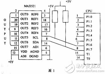
OUT0~OUT7: voltage output terminals of DAC0~7; REF0~REF3: reference voltage input terminals of DAC0~3; REF4: reference voltage input terminals of DAC4~7; AD0, AD1: device address input pin; SCL: serial Clock input; SDA: serial data input; DGND: digital signal ground; AGND: analog signal ground
2 MAX521 software communication protocol
I2C bus composition: consists of only two lines. One is the clock line (SCL) and the other is the data line (SDA). The SCL line is a clock signal that is generated by the bus control device to provide a uniform clock signal to the bus.
The SDA line is a data signal that is transmitted bidirectionally between the bus control device and other devices on the bus.
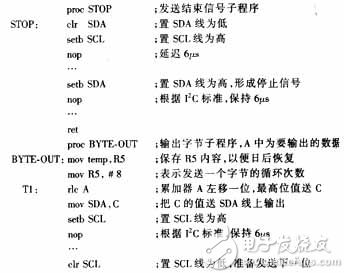
The I2C bus protocol specifies that the SDA signal is active when SCL is high and the data change on the SDA line should be performed when SCL is low. The only exceptions to this rule are the start signal and the stop signal.
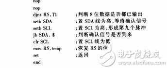
The format of the I2C input/output one byte is the high bit first and the low bit last. Each I2C bus access is made up of a series of basic operations, which are explained in detail below.
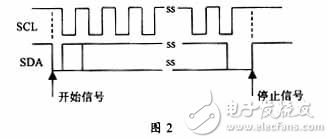
2.1 start signal
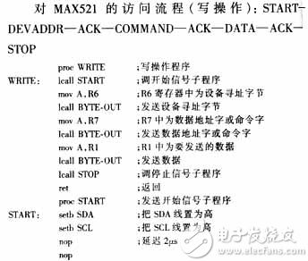
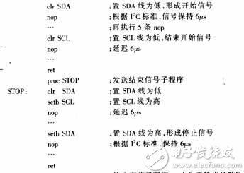
The start signal is sent on the bus before each I2C bus access. When the SCL line is high, the SDA line goes from high to low, and a start signal is formed.
2.2 End signal
The end signal is sent on the bus after each I2C bus access. When the SCL line is high, the SDA line goes from low to high, and an end signal is formed.
The timing diagrams for the start and stop signals are as follows:
2.3 device addressing byte
A device addressing byte is required for both read and write operations. The first five bits of the MAX521's addressed byte are 01010 (the device's flag code is selected). The last two bits are the device address, which is determined by the state of the AD521 and AD1 pins of the MAX521. The last bit X is to write or read data to the device. If data is written to MAX521, X is 0.
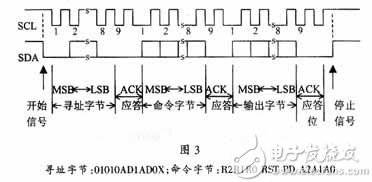
Below is a complete working timing diagram for the MAX521:
2.4 data address byte or command byte
The device addresses the byte followed by the command word. The first three bits of the command word are 0, the last two bits are RST and PD, and the next three bits A2A1A0 are the channel addresses of the eight DAC output registers. The working sequence of the data address byte or command byte is shown in Figure 4:
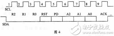
R2R1R0 is set to 0 and is a reserved bit. When RST is high, the MAX521 resets all DAC registers, but the output remains asserted until the Stop signal. When the PD bit is high, the MAX521 enters a low power mode after receiving a "stop signal". In low-power mode, the DAC output is dependent on the channel address setting and output byte setting state at this time, providing a maximum current of 20μA. When the PD bit is low, the MAX521 returns to normal operation and then sends a “stop signalâ€. The voltage output from the DAC depends on the current channel address setting and output byte settings.
2.5 response signal
During each ninth clock pulse after each address byte or one data byte is transmitted, the receiver generates a low-level acknowledge signal ACK on the SDA line to inform the sender that the data has been received and can continue to transmit. . After all the data is transferred, the MCU sends a stop signal to the SDA line to end the data transfer.
note:
1) When the bus is idle, the SCL and SDA lines should be held high.
2) The bus idle time tBUF>4.7μs before a new start.
3) The time when the clock is high level and low level and the start time of the start signal and the end signal are established must be greater than 4.7μs.
4) Two write transmission time intervals tWR>10ms.
5) The operating rate of the SCL line can reach 400 kHz.
3 MAX521 and MCU interface and program
As shown in Figure 1, the MAX521 is connected to P1.6 and P1.7 of the microcontroller and operates as an I2C bus. All reference voltages are connected to +5V, so that the analog voltage value of the output is between 0 and +5V. The device address is set to 01B. OUTPUT is followed by the execution device.
4 Conclusion
This system has been successfully applied in circuits with multiple DAC conversions, which is more than the cost of the usual parallel DAC devices, and provides a good solution for intelligent device development.
To satisfy high voltage application demands, allowing apm DC Source System to cover a voltage range from 0V to 800V,the switching power supply has low load regulation, which ensure stable output when the load is changing constantly. The smps power supply supports standard SCPI communication protocol, which is convenient for user`s secondary development.
Some features as below:
- With accurate voltage and current measurement capability.
- Coded Knob, multifunctional keyboard.
- Standard RS232/RS485/USB/LAN communication interfaces, GPIB is optional.
- Remote sensing line voltage drop compensation.
- Equips with LIST waveform editing function.
- Use the Standard Commands for Programmable Instrumentation(SCPI) communication protocol.
- Have obtained CE certification.
800V DC Source System,Adjustable Voltage Power Supply,Dc Voltage Source,800V Dc Power Source
APM Technologies Ltd , https://www.apmpowersupply.com