Abstract: VS1001K is a new MP3 decoder chip produced by VLSI SoluTIon of Finland. The chip contains high-quality stereo digital-to-analog converter (DAC) and headphone drive circuit, supporting PCM data input. It also has the advantages of small size, low power consumption, simple interface and cheap price. The article introduces the pin arrangement, internal structure and main features of VS1001K. At the same time, the functions and addresses of the registers in the SCI control interface of the VS1001K and the operation method of the SDI data interface are mainly introduced. Finally, the application circuit of VS1001K is given.
1 Introduction 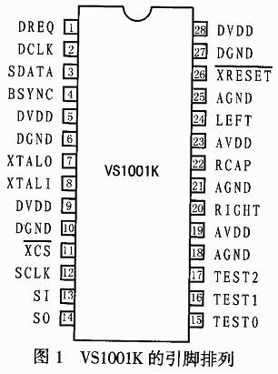
At present, the MP3 audio data compression method used by INTERNET and portable players has become a recognized industry standard. This method quickly became popular all over the world due to its high compression ratio and good sound quality. But in fact, the core of many MP3 players is a MP3 audio decoding chip. VS1001K is a new MP3 decoder chip launched by Finland VLSI Solution. The chip contains high-quality stereo digital-to-analog converter (DAC) and headphone driver circuit, it supports PCM data input, and has the advantages of small size, low power consumption, simple interface, cheap price and so on. Therefore, it is expected to become the chip of choice for the new MP3 decoder.
2 Functional structure of VS100K
2.1 Pin function of VS100K
VS1001K has two package types: 28-pin SOIC dual-row and 49-pin BGA ball grid array. Figure 1 shows the pin layout of the 28-pin SOIC package. The specific function description of each pin is listed in Table 1.
Table 1 VS1001K pin functions
| Pin number | Pin name | Features |
| 1 | DREQ | Data request port |
| 2 | DCLK | SDI clock signal input |
| 3 | SDATA | SDI data input |
| 4 | BSYNC | Byte sync signal |
| 5, 9, 28 | DVDD | Digital power |
| 6, 10, 27 | DGND | Digitally |
| 7 | XTALO | Clock signal output |
| 8 | XTALI | Clock signal input |
| 11 | XCS | Chip select, active low |
| 12 | SCLK | SCI clock input |
| 13 | SI | SCI data input |
| 14 | SO | SCI data output |
| 15 ~ 17 | TEST0 | Alternate test port |
| 18, 21, 25 | AGND | Simulated |
| 19, 23 | AVDD | Analog power |
| 20 | RIGHT | Right channel audio output |
| twenty two | RCAP | External capacitor access terminal |
| twenty four | LEFT | Left channel audio output |
| 26 | XRESET | Circuit reset terminal, active low |
Table 2 SCI register functions
| Register name | Address | Types of | Features |
| MODE | 0x00 | RW | Used to control the operation of VS1001K |
| STATUS | 0x01 | RW | Current status information of VS1001K |
| INT_FCTLH | 0x02 | - | Internal registers, generally not used |
| CLOCKF | 0x03 | RW | Control clock frequency and frequency multiplier |
| DECODE_TIME | 0x04 | R | Determine the decoding time (in seconds) |
| AUDATA | 0x05 | R | Sound data |
| WRAM | 0x06 | W | Used to write user program to program RAM |
| WRAMADDR | 0x07 | W | Set the base address for WRAM operation |
| HDAT0 | 0x08 | R | Read MP3 header data |
| HDAT1 | 0x09 | R | Read MP3 header data |
| A1ADDR | 0x0A | RW | Determine the start address of the user application |
| VOL | 0x0B | RW | Used for volume control, high and low bytes are left and right channels respectively. The volume ranges from 0 to FF, with 0 being the largest and FF being the smallest |
| RESERVED | 0x0C | - | Keep |
| A1CTRL [0] | 0x0D | RW | Used to control user applications |
| A1CTRL [1] | 0x0E | RW | Used to control user applications |
2.2 The internal structure of VS100K
The VS100K decoder chip integrates the VS DSP processor, and it also integrates stereo audio DAC, stereo headphone amplifier driver, and program ROM and program RAM. In addition, VS100K also has a serial data interface and control interface. Figure 2 is a block diagram of the internal structure of VS100K. 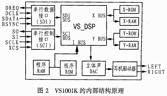
3 Working principle of VS100K
VS1001K mainly receives the external microprocessor to control commands and MP3 data through two serial interfaces SCI and SDI. Among them, SCI is used to receive control commands sent by external microprocessors, and SDI is used to receive MP3 data sent by external microprocessors.
3.1 SCI control interface
The control of VS100K is mainly achieved by operating 15 16-bit registers in SCI. Table 2 lists the names, addresses, types and functions of 15 16-bit registers of SCI. In fact, the main operation of the VS100K is done through the MODE register. Table 3 gives a description of the operating functions of the MODE register.
Table 3 MODE register operation method
| Bit | Name | Features | Instructions |
| 0 | SM_DIFF | Differential output control | 0 is normal, 1 is left channel inversion |
| 1 | SM_FFWD | Fast forward | 0 is normal speed, 1 is fast forward |
| 2 | SM_RESET | Software reset | 0 is not reset, 1 is reset |
| 3 | SM_MP12 | Whether to decode MP1 and 2 | 0 is for MP3 only, and MP1 / 2/3 is decoded when 1. |
| 4 | SM_PDOWN | Power-down control | 0 is power on, 1 is power off |
| 5 | SM_DAC | Digital-to-analog mode control | 0 is general MPEG decoding, 1 is PCM decoding |
| 6 | SM_DACMONO | Stereo digital-to-analog conversion control | 0 is stereo, 1 is mono |
| 7 | SM_BASS | High / bass booster | 0 is off, 1 is on |
| 8 | SM_DACT | DCLK trigger edge | 0 is from MSB, 1 is from LSB |
| 9 | SM_BYTEORD | Byte transfer order | 0 is a rising edge, 1 is a falling edge |
| 10 | SM_IBMODE | Operating mode | 0 is slave mode, 1 is master mode |
| 11 | SM_IBCLK | VS1001K is used for DCLK frequency setting when working in master mode | Choose 512kHz at 0, 1024kHz at 1 |
The communication protocol between SCI and external microprocessor includes instruction byte, address byte and 16-bit word. Among them, the instruction byte takes 0X03 as a read register and 0X02 as a write register; the main purpose of the address byte is to determine the address of the address register, and its range is 0X00 ~ 0X0E. The 16-bit word is used to point to the value written or read from the specified register. Figure 3 shows the timing of the read and write operations of the SCI register.
3.2 SDI data interface
When the external microprocessor transmits MP3 data to the VS100K through the SDI interface, under different settings of the MODE register, the SDI can work in both master and slave modes.
When SDI works in master mode, its DClk signal is generated internally by VS100K (specifically, 512kHz or 1024kHz is determined by the SM IBCLK bit in the MODE register), and when SDI works in slave mode, DClk is input externally.
SDI usually carries on the data transmission in the unit of byte, and input the SATA data signal on the rising or falling edge of the DCLK (specifically determined by the SM_DACT bit in the MODE register). Whether the high bit is first or the low bit is first used in data transfer is determined by the SM DAC bit of the MODE register. SDI uses BSYNC signals to ensure that there is no misalignment during data transmission.
Figure 3, Figure 4
When SDI receives data in slave mode, if there is enough space in the on-chip FIFO, VS1001K will issue a high-level DREQ data request signal to indicate that it can receive at least 32 bytes of MP3 data.
4 Application of VS100K
Fig. 4 is the application circuit that VS100K connects with external microprocessor through SDI and SCI interface. As can be seen from the figure, because the VS100K decoder has integrated a digital-to-analog converter and an audio drive circuit for headphones in its chip, its peripheral circuit is very simple. In fact, the circuit in Figure 4 has been optimized for the interface circuit between VS100K and the microprocessor.
Regarding the software programming of reading and writing SCI registers or transferring MP3 data to SDI, the software programming may be different for different external microprocessors. But neither is very complicated. Due to space limitations, this article will not repeat them.

Follow WeChat

Download Audiophile APP

Follow the audiophile class
related suggestion
Abstract: ADV7183 is an enhanced video decoder with 10-bit ADC integrated by American Analog Devices (ADI). Inside it ...
Abstract: IME6400 is an integrated circuit developed by South Korean INTiME that can support MPEG4 high-resolution real-time video encoding ...
Three-terminal ...
![[Photo] Three-terminal voltage regulator XWY2005 and its application](http://i.bosscdn.com/blog/20/06/41/7212011242.jpg)
...
High Accuracy CMOS Operational A ...
![[Photo] High-precision CMOS operational amplifier LMC6062 / ...](http://i.bosscdn.com/blog/20/06/41/6175842568.gif)
Abstract: NCP1
![[Photo] Single-ended PWM controller NCP1205 and its application](http://i.bosscdn.com/blog/20/06/41/6173136914.gif)
NE605 is Philips ...
![[Photo] High performance small power FM receiver chip NE605 and its application ...](http://i.bosscdn.com/blog/20/06/41/5192033610.gif)
Abstract: TDA9332H is a display processor suitable for high-end color TV produced by Philips, which can be used for single scan (50 or 60Hz) and dual ...
Introduction
Abstract: The parallel interface high-performance ferroelectric memory FM1808 produced by RAMTRON is an ideal substitute for NV-SRAM ...
Abstract: Introduces the features of the zero-power ultra-fast and complex programming logic device ispMACH4000Z introduced by Lattice Semiconductor, ...
This article introduces the main features, pin functions, software design, hardware connection and specific application circuit of PTR2030. PTR2030 is super ...
XTR110 is a precision voltage / current converter launched by Burr-Brown Company of the United States. It is designed for analog signal transmission ...
Abstract: This article introduces the MAX712 / MAX713 programmable battery charge management chip produced by MAXIM, using MAX ...
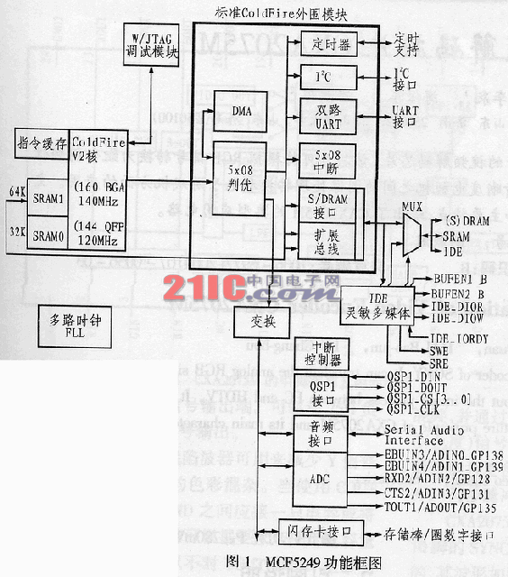
Abstract: This article introduces the principle, characteristics and pin functions of the embedded microprocessor MCF5249 of MOTOROLA company, and explains ...
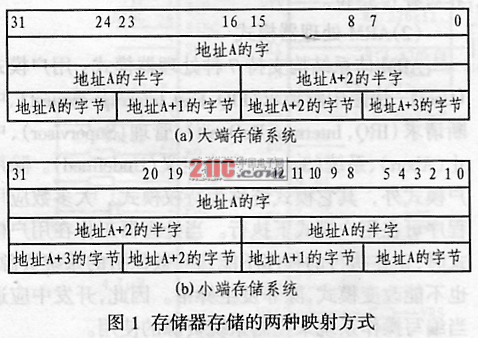
Abstract: Based on the analysis of the ARM architecture, the structural characteristics and advantages of the 32-bit ARM core processor W90N740 are introduced ...
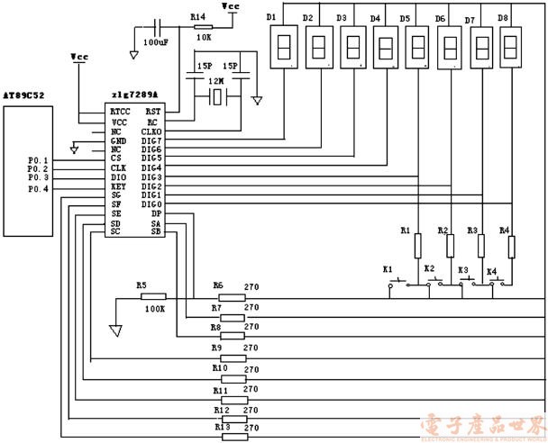
Abstract: This article introduces in detail the basic principles, features and original use of the digital tube and keyboard smart chip zlg7289A ...
Abstract: This article introduces the structure, function and interface characteristics of OMAP5910, and ...

Abstract: CS6208 is a chip specially developed by Myson Century for network control and transmission. It is based on 80 ...
