Abstract: TDA9332H is a display processor suitable for high-end color TVs produced by Philips. It can be used for single-scan (50 or 60 Hz) and dual-scan (100 or 120 Hz) TV signal processing. The article introduces the structure principle and performance characteristics of TDA9332H, and also gives the application method of TDA9332H in high-end color TV.
1 Main features of TDA9332H
TDA9332H is a display processor designed by Philips for high-end color TVs. It uses a 44-pin QFP package, and its pinout is shown in Figure 1. In addition, the chip has the following characteristics:
â— It has YUV input terminal and RGB signal input terminal with fast blanking, its OSD / Text input terminal is separated from other video signal input terminals, and it has both fast blanking function and mixed insertion; it also has built-in RGB control processor , Can implement continuous cathode correction (CCC), white point and black level shift adjustment; can provide stable black current RGB output; can effectively solve the defects such as color cast and contrast reduction of CRT display image caused by too long use time .
â— Programmable deflection processor capable of generating internal clock. These drive signals include line drive, field deflection, and parabolic wave corrected by east-west. The circuit can be adapted to both 4: 3 CRT and 16: 9 CRT.
â— It can be used for single scan (50 Hz or 60 Hz) or double scan (100 Hz or 120 Hz).
â— The internal clock generator used for line and field deflection processing can be synchronized by a 12MHz ceramic resonator, thereby improving the timing accuracy of the line and field deflection processing circuit.
â— Horizontal synchronization circuit with two control loops, and the horizontal oscillator does not need to be adjusted; the horizontal drive pulse can implement slow start and slow stop; it has the ability to process line and field geometric distortion and horizontal parallelogram and bow correction. 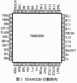
â— The built-in blue extension circuit can shift the near-white color to the blue side, so as to improve the brightness of the white field of the image.
â— It also has a black level extension processing function for non-standard brightness signals, so that the video signals input from different sources have a consistent image level after being processed by the circuit; at the same time, the device also has a switchable to adapt to the color difference signal Matrix, can be applied to the processing and display of multi-standard color difference signals;
â— With horizontal and vertical zoom function, and vertical scroll frame function suitable for 16: 9 picture tube.
â— The power supply voltage of this chip is + 8V, the total power supply current is 50mA, and all functions inside the chip can be controlled by the I2C bus.
2 Pin function and internal structure
TDA9332H has 44 pins, and the functions of each pin are listed in Table 1. Figure 2 shows a block diagram of its internal structure.
Table 1 TDA9332H pin functions
| Pin identification | Pin number | Pin function description | Pin identification | Pin number | Pin function description |
| VDOA | 1 | Field sawtooth wave output A after geometric correction | VD | twenty three | Field sync input |
| VDOB | 2 | Field sawtooth wave output B after geometric correction | HD | twenty four | Line sync input |
| EWO | 3 | East-west pillow output | DACOUT | 25 | DAC output |
| EHTIN | 4 | High voltage stable detection signal output | VIN | 26 | V signal input |
| FLASH | 5 | Quick input detection | UIN | 27 | U signal input |
| GND1 | 6 | Ground | YIN | 28 | Y signal input |
| DECVD | 7 | Digital power filter | FBCSO | 29 | Fixed beam current shutdown input |
| HOUT | 8 | Line excitation pulse output | RI1 | 30 | Red primary color signal 1 insertion |
| SCO | 9 | Sandcastle pulse output | GI1 | 31 | Green primary signal 1 insertion |
| SCL | 10 | I2C bus clock line | BI1 | 32 | Blue primary color signal 1 insertion |
| SDA | 11 | I2C bus data line | BL1 | 33 | Fast blanking 1 insert |
| HSEL | 12 | Line frequency selection control | PWL | 34 | Baifeng limiting decoupling |
| HFB | 13 | Line backward pulse input | RI2 | 35 | Red primary signal 2 insertion |
| DPC | 14 | Dynamic phase compensation | GI2 | 36 | Green primary signal 2 insertion |
| VSC | 15 | Field sawtooth wave is formed, external sawtooth wave forms capacitor | BI2 | 37 | Blue primary color signal 2 insertion |
| IREF | 16 | Field sawtooth wave forming reference current setting | BL2 | 38 | Fast blanking 2 insertion |
| VPI | 17 | + 8V power supply (line start) | VP2 | 39 | + 8V power supply |
| DECBG | 18 | Power regulator filter capacitor connection (band gap filter) | RO | 40 | Red primary color signal output |
| GND2 | 19 | Ground | GO | 41 | Green primary color signal output |
| XTALI | 20 | 12MHz crystal input | BO | 42 | Blue primary color signal output |
| XTALO | twenty one | 12MHz crystal output | BCL | 43 | Beam current limit input |
| LPSU | twenty two | Low voltage start circuit power supply | BLKIN | 44 | Black current detection input |
3 The working principle of TDA9332H
3.1 Selection and display processing of image signal
The selection and display processing of the image signal in TDA 9332H includes the conversion of RGB signals into YUV signals, YUV selection, black level extension and chromaticity control, primary color matrix, contrast control, primary color signal selection, white peak and brightness control, peak limiting and beam current Control, automatic adjustment of dark balance, blue level extension and output amplification. The TDA9332H has three signal input ports, namely a YUV and two RGB input ports. The YUV input port is used to output the YUV signal for the field multiplication / progressive processing section.
Among the above three input ports, the first RGB input port is used for external video RGB signal input, and the second RGB input port is used for OSD and teletext RGB signal input. The signal conversion of the three input ports is controlled by the microprocessor through the I2C bus.
The processing of RGB output signals includes white peak limiting, beam current limitation, continuous calibration of cathode beam current, blue level extension and other circuits.
3.2 Synchronization, deflection small signal processing and geometric distortion correction
figure 2
(1) Clock generator and first phase-locked loop
The clock generator in the TDA 9332H consists of a voltage-controlled oscillator and the first phase-locked loop to generate the clock signal required for synchronization and deflection processing. The free oscillation frequency of the voltage-controlled oscillator is 880 times the input signal line frequency (1fH mode) Or 440 times (2fH mode). The frequency of the internal voltage-controlled oscillator is determined by the input line synchronization signal and the control potential of the mode selection terminal.
(2) Working principle of the second phase-locked loop and horizontal phase shift
After the voltage-controlled oscillator is divided by 880 or 440, the obtained 1fH or 2fH line excitation signal is sent to the second phase-locked loop for phase discrimination with the line reverse pulse. The error signal is used to control the phase of the line excitation pulse after internal filtering, and it can also be used to correct the horizontal phase shift of the image caused by the beam current change.
In order to correct the line width change caused by the beam current change, the TDA9332H also sets a dynamic line width fine-tuning function. When the sampling voltage of dynamic line amplitude fine-tuning is introduced from one end of the high-voltage winding of the line output transformer to the 14 feet of TDA 9332H through the resistance, the beam current change will cause the potential change of this pin, and the internal correction circuit can automatically adjust according to the potential change of this point Reverse pulse phase of the second phase-detection loop. When the beam current increases, the output of the second phase-detection loop will reduce the line width, otherwise, the line width will increase, thereby achieving the purpose of automatically fine-tuning the line width with the beam current size.
Within TDA9332H, the error control voltage output by the second phase-locked loop can be changed through the I2C bus data to achieve the effect adjustment of the image in the horizontal direction; the effect adjustment is based on the vertical deflection center as the reference point, using up and down respectively The scanning lines of the two halves are implemented by increasing the phase shift line by line.
(3) Geometric distortion correction
The field geometry correction circuit built in TDA9332H can implement field amplitude adjustment, S-shape correction, field slope correction, field offset and field zoom, field roll frame (that is, when the field scan expands, the graphics can be moved in the vertical direction), field waiting ( That is, the starting point of field scanning can be adjusted with delay) and other functions.
TDA 9332H's east-west geometric correction includes line width increase range, east-west corner and parabolic wave ratio, east-west corner and parabolic wave ratio, and east-west trapezoidal distortion according to zoom performance.
TDA9332H also has an EHT compensation input signal, which can be used to control the field and E-W output signals, and can also adjust the relative control effect of the two via the I2C bus.
4. Application of TDA9332H in high-end color TV 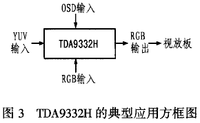
Figure 3 shows the typical application block diagram of TDA9332H in high-end TV. The ordinary TV signal is converted into frequency multiplier or progressive Y, U, V signal by the scan rate converter, and this signal is added to the 26, 27, 28 pin of TDA 9332H, and then the R, G output from the high definition digital TV set-top box , B signal or the R, G, B signal output from the PC is added to the 30, 31, 32 pins of TDA9332H, and then this signal is processed by the internal RGB-YUV matrix and the video component signal switch, and thus select a TV signals. After the R, G, B and blanking signals of the OSD are input from pins 35, 36, 37 and 38, they are mixed with the incoming main TV signal, and then the white point and brightness control and output buffering are carried out, and then by 40, 41, The 42-pin output is divided into three channels and transmitted to the 32MHz bandwidth of the final stage TV amplifier TDA6120Q for power amplification, and finally added to the cathode of the kinescope.
In order to improve the image quality, TDA 9332H also added a black level extension circuit, blue level extension circuit, white peak limiter and automatic brightness control circuit. The ABL voltage detected by the high-voltage winding of the line-reverse transformer is amplified by the triode and applied to pin 43; and the black current calibration voltage detected by the final stage of the reflex that reflects the change in CRT cathode current is applied to pin 44 to automatically adjust the brightness of CRT calibration.
5 Conclusion
Because all functions of TDA9332H are controlled by I2C bus, and the application is simple, few peripheral components, low power consumption and high cost performance. Therefore, the chip has been more and more widely used in various high-end TVs such as progressive color TV and digital high-definition TV.

Follow WeChat

Download Audiophile APP

Follow the audiophile class
related suggestion
The design and implementation of keyboard driver based on I2C bus With the rapid development of embedded systems, embedded PC has been widely used in many fields. ...
Abstract: ADV7183 is an enhanced video decoder with 10-bit ADC integrated by American Analog Devices (ADI). Inside it ...
Abstract: IME6400 is an integrated circuit developed by South Korean INTiME that can support MPEG4 high-resolution real-time video encoding ...
I2C bus is the abbreviation corresponding to (Inter IC BUS), which is Ph ...
Most large-screen color TVs are now I2C bus color TVs. Once a failure occurs, ...
Three-terminal ...
![[Photo] Three-terminal voltage regulator XWY2005 and its application](http://i.bosscdn.com/blog/20/06/41/7212011242.jpg)
...
High Accuracy CMOS Operational A ...
![[Photo] High-precision CMOS operational amplifier LMC6062 / ...](http://i.bosscdn.com/blog/20/06/41/6175842568.gif)
Abstract: NCP1
![[Photo] Single-ended PWM controller NCP1205 and its application](http://i.bosscdn.com/blog/20/06/41/6173136914.gif)
NE605 is Philips ...
![[Photo] High performance small power FM receiver chip NE605 and its application ...](http://i.bosscdn.com/blog/20/06/41/5192033610.gif)
Abstract: VS1001K is a new MP3 decoder chip produced by VLSI Solution of Finland. The chip contains high quality ...
Introduction

Abstract: The parallel interface high-performance ferroelectric memory FM1808 produced by RAMTRON is an ideal substitute for NV-SRAM ...
Abstract: Introduces the features of the zero-power ultra-fast and complex programming logic device ispMACH4000Z introduced by Lattice Semiconductor, ...
This article introduces the main features, pin functions, software design, hardware connection and specific application circuit of PTR2030. PTR2030 is super ...
XTR110 is a precision voltage / current converter launched by Burr-Brown Company of the United States. It is designed for analog signal transmission ...
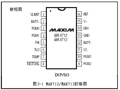
Abstract: This article introduces the MAX712 / MAX713 programmable battery charge management chip produced by MAXIM, using MAX ...
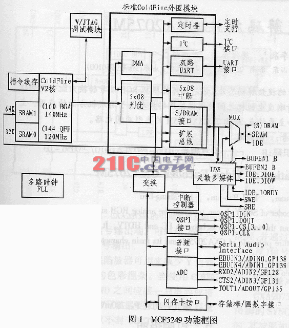
Abstract: This article introduces the principle, characteristics and pin functions of the embedded microprocessor MCF5249 of MOTOROLA company, and explains ...
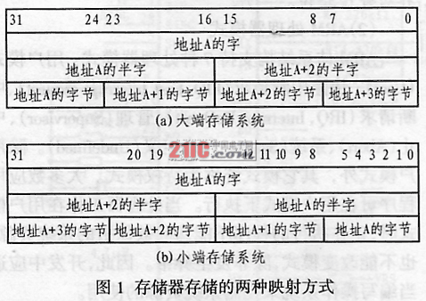
Abstract: Based on the analysis of the ARM architecture, the structural characteristics and advantages of the 32-bit ARM core processor W90N740 are introduced ...
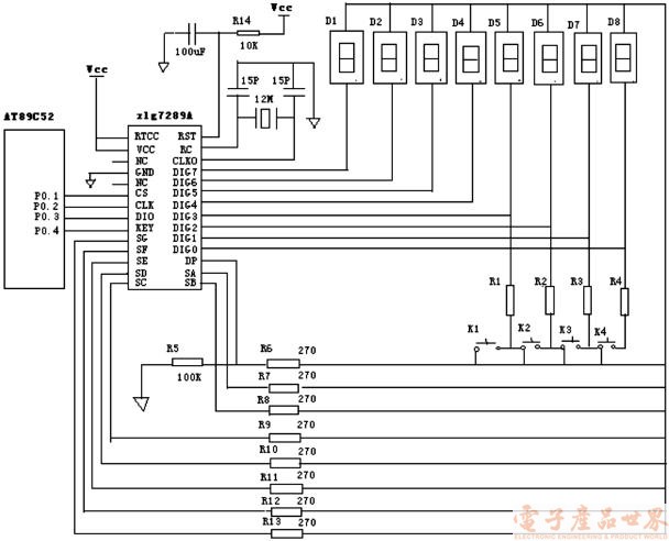
Abstract: This article introduces in detail the basic principles, features and original use of the digital tube and keyboard smart chip zlg7289A ...
Abstract: This article introduces the structure, function and interface characteristics of OMAP5910, and ...

Abstract: CS6208 is a chip specially developed by Myson Century for network control and transmission. It is based on 80 ...
