Among the well-known materials, Ferroelectric gate field-effect transistors (FeFETs) are promising for a new generation of flash memory.
The momentum of a new generation of ferroelectric memory is emerging, which will change the next generation of storage.
Typically, ferroelectrics are associated with a type of memory, ferroelectric RAMs (FRAMs). In the late 1990s, FRAMs introduced by several vendors were low-power, non-volatile devices, but they were also limited to niche applications and could not be extended beyond 130 nm.
While FRAM continues to be produced, the industry is also developing another type of ferroelectric memory. FeFET and related technologies do not use the materials used in conventional FRAM, but utilize the ferroelectric properties of yttrium oxide (also known as ferroelectric oxide). (FeFET is different from logic transistor FinFET).
However, as far as the development phase is concerned, FeFET itself is not a new device. For FeFET, the main principle is to use a yttrium-based High-K (high-K) gate dielectric + Metal Gate electrode stacking technique on existing logic transistors, and then modify the gate insulator to have Ferroelectric properties. The resulting FeFET transistors have the same structure but are scalable, low power, and non-volatile. In theory, it should be better than current embedded flash.
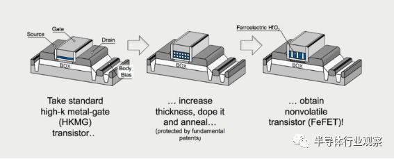
Figure 1: FeFET production process.
Many researchers are working on different types of FeFET-based nonvolatile devices. This sounds like a simple concept, but there are several key challenges such as integration, data retention, reliability and cost. Greg Wong, an analyst at Forward Insights, said: "FeFETs are promising, but it's too early."
Of course there are other challenges. Ferroelectric Memory Co. (FMC) is developing FeFET, its CEO Stefan Müller said: "For the emerging memory technology, the hardest part is to make sure that your solution is true and reliable."
Despite this, FeFET and its related technologies are booming. Here are the latest developments:
• GlobalFoundries, FMC, NaMLab, Fraunhofer, etc. have demonstrated an embedded non-volatile FeFET in the 22nm FD-SOI process, which has achieved an important milestone. Although there is no production schedule, the technology will be certified in 2019.
• Imec is developing a solution to replace current DRAM materials with ferroelectric oxides to create a new class of non-volatile DRAM-like memories. In addition, Imec is also developing stacked ferroelectric devices similar to 3D NAND.
• SK Hynix, Lam Research, Versum, etc. recently published a paper on the switching mechanism of such devices, one of which is called 1T-FeRAM and a 3D FeNAND.
• More and more teams are exploring the next generation of ferroelectric oxide-based logic transistor types, often referred to as negative capacitance field effect transistors (NC-FETs). NC-FETs are potential technologies for transistors of 3 nm and above.
3D FeNAND, ferroelectric DRAM and NC-FET are still in the early stages of development, and it is too early to say whether these technologies can be put into production. Companies such as GlobalFoundries and FMC are large test sites for the development of FeFET.
If it succeeds, FeFET will enter the crowded field of the next generation memory market. Other new memory types, such as 3D XPoint, Magnetoresistive RAM, ReRAM and even traditional FRAM, are shipping. To a large extent, FeFET will compete with some of these technologies.
Next generation memory contest
The industry has been developing the next generation of memory types for many years, for the simple reason that traditional memory has various limitations.
For example, DRAM used as the system's main memory is fast and cheap, but DRAM loses data when the system is powered off.
NAND and NOR flash are also very cheap. Flash is non-volatile and can store data even when the power is off. However, in operation, the flash will go through several read/write cycles, which is a slow process.
This is where new flash is available. In general, next-generation memory types are fast, non-volatile, and offer unlimited endurance. They also offer variable bit, no erase capability, making them an ideal replacement for DRAM and flash memory. But these new memories also depend on exotic materials and complex conversion mechanisms, so they take longer to develop. At the same time, the industry continues to expand the size of DRAM and flash memory, making it difficult for new memory types to gain a foothold in the market.
However, some new types of memory in the industry are beginning to increase. Here's a simple picture:
• Intel and Micron are introducing next-generation 3D XPoint technology based on phase change memory. The 3D XPoint is a stand-alone device that accelerates the operation of solid state drives (SSDs).
• Everspin and others are developing next-generation MRAM technology from spin-torque magnetoresistive RAM (STT-MRAM). STT-MRAM is used in embedded or stand-alone applications, and the magnetic properties generated by electron spin provide non-volatility in the chip.
• Several vendors and foundries are developing resistive RAM (ReRAM) for stand-alone embedded applications. In ReRAM, a voltage is applied to the material stack to record the data resulting from the change in resistance.
• Cypress, Fujitsu, Panasonic, Texas Instruments and others are introducing microcontrollers (MCUs) with embedded FRAM.
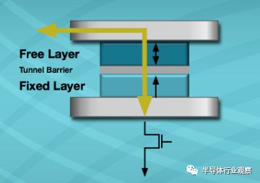
Figure 2: Spin Torque MRAM Technology.
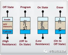
Figure 3: ReRAM.
FRAM is widely misunderstood because ferroelectric materials are not ferromagnetic. FMC's Müller explained: "The ferroelectric memory uses only the electric field to write to the application and no current flows. All other emerging memories, such as resistive RAM, phase change memory and MRAM, are driven by the current in the memory cell. To write.
FRAM uses the ferroelectric effect of ferroelectric crystals to achieve data storage. The ferroelectric effect means that when a certain electric field is applied to the ferroelectric crystal, the central atom of the crystal moves under the action of the electric field and reaches a stable state; when the electric field is removed from the crystal, the central atom will remain in the original position. This is because the middle layer of the crystal is a high energy level, and the central atom cannot cross the high energy level to reach another stable position when no external energy is obtained. Therefore, the FRAM does not require voltage to maintain data, and does not need to be periodically refreshed like DRAM. Since the ferroelectric effect is a polarization polarization characteristic inherent to ferroelectric crystals, it is independent of electromagnetic action, so the content of the FRAM memory is not affected by external conditions (such as magnetic field factors), and can be used like ordinary ROM memories. Non-volatile storage features and unlimited durability make them ideal for a wide range of embedded chip applications.
Typically, FRAM consists of a thin layer ferroelectric thin film based on lead zirconate titanate (PZT). According to Cypress, the atoms in PZT change polarity in the electric field to form a power-efficient binary switch.
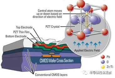
Figure 4: Traditional FRAM
However, FRAM has some problems. Muller said: "Classic FRAM is unusual from a material point of view. Since only planar capacitors can be used, traditional ferroelectric films are not expandable, and FRAM does not exceed the 130 nm technology node. This prevents traditional FRAM from being widely used. use."
Since FeFET is different from traditional FRAM, supporters hope to solve these problems. A few years ago, the industry had a new discovery, the ferroelectric properties of bismuth oxide. The researchers found that the crystal phase can be stabilized during the doping of yttrium oxide. According to FMC, "In this crystal phase, the oxygen atoms of yttrium oxide can exist in two stable positions, moving up or down according to the polarity of the applied electric field."
Cerium oxide is a well-known material. For some time, chip manufacturers have used yttrium oxide as a gate stack material for high-k/metal gate structures in logic devices of 28 nm and above. For FeFETs, the characteristics of ferroelectric oxides are mainly used instead of using special materials to create new device structures.
For example, in the FMC technology, it is desirable to use existing transistors. A silicon-doped yttria material is then deposited into the gate stack of the transistor using a deposition process to produce ferroelectric properties. The FMC solution also eliminates the need for capacitors, making single-transistor memory cells or 1T-FeFET technology possible.
Müller said: "In FeFET, the permanent dipole is formed in its own internal gate dielectric, which divides the threshold voltage of the ferroelectric transistor into two stable states. Therefore, the binary state can be stored in the FeFET, just like in a flash memory cell. The same."

Figure 5: FeFET (n-type): When the iron is polarized down (left), the electrons reverse the channel region, permanently putting the FeFET into an "on" state. If the polarization point is up (middle), it accumulates permanently and the FeFET is in the "off" state. Source: FMC.
In theory, the technology is convincing. “Each cutting-edge transistor has yttrium oxide. This is the gate dielectric. If you do this ingeniously and modify yttrium oxide, you can actually convert the logic transistor into a non-volatile transistor that is disconnected. A state is lost when the power is turned on. It can still be maintained after the power is turned off."
FeFET is still in the research and development stage and is not ready for the golden age. But if it does, consumers have another option in the next generation of flash memory. 3D XPoint, FRAM, MRAM, ReRAM, etc. are also in the alternative.
So, what new memory technology will prevail? This is not clear because there is no single memory that can handle all the requirements. Each new memory type has its own characteristics. New memories are eroding some markets from traditional memories. But in general, traditional DRAM and NAND continue to dominate at the memory level.
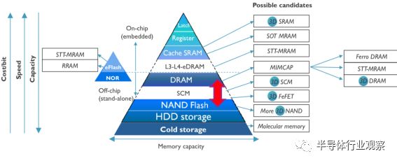
Figure 6: Memory Pyramid
Embedded memory war
In terms of storage space, emerging battlefields are forming in the embedded market. Today's MCUs integrate multiple components on the same chip, such as CPU, SRAM, and embedded memory. The CPU is responsible for executing the instructions. SRAM is integrated on the chip to store data.
Embedded memories such as EEPROM and NOR flash are used for code storage and other functions. Objective Analysis analyst Jim Handy said in a recent interview: "With EEPROM, each byte is two transistors. Each byte can be erased or reprogrammed. On each module (NOR flash) We have a huge transistor that erases all bytes. Compared to two transistors per byte, huge transistors can still save a lot of chip space."
Embedded Flash (eFlash) is powerful enough for industrial applications. For example, automotive OEMs have strict requirements, and NOR also meets this requirement. Walter Ng, vice president of US sales for UMC, said: "The car MCU is driven by performance, which is the driving force of eFlash.
NOR has some limitations because the write speed is very slow. It has also become more and more expensive to move the NOR from 40 nm to 28 nm. It is unclear whether NOR can be extended to more than 28nm.
The next generation of flash memory suppliers hope to fill the gap. Emerging RAM seems to offer a possible solution. However, it remains to be seen how the automotive industry will accept such technology. â€
In any case, the embedded memory market is heating up. Several foundries such as GlobalFoundries, Samsung, TSMC and UMC are developing embedded STT-MRAM. In addition, SMIC, TSMC and UMC are also developing embedded ReRAM.
FeFET is a new product in this field. In 2009, Fraunhofer, GlobalFoundries and NaMLab began exploring FeFET. Later, FMC became independent from NaMLab.
In 2014, the team demonstrated a simple FeFET array based on a 28nm CMOS process. Then, at the recent IEDM conference, GlobalFoundries, Fraunhofer, NaMLab and FMC presented new results that made FeFET closer to commercialization.
The team demonstrated embedded FeFETs in the 22nm FD-SOI process. Gary Patton, chief technology officer at GlobalFoundries, said: "The way to make very dense memory is relatively low cost."
According to the IEDM paper, the cell size of the FeFET is as small as 0.025 μm 2 . The device consists of a 32MB array with a program/erase pulse in the 10ns range of 4.2V. It has a holding rate of up to 300 °C.
Initially, FeFET's goal was to target the embedded non-volatile memory market for consumer applications. "Write speed is about two orders of magnitude faster than traditional eFlash. We are at 10ns, regime is between 1ms and 10ms," FMC's Muller said.
Technology is possible. Imec outstanding technician Jan Van Houdt said: "They are going further than others. They are now advancing embedded solutions, which may work."
FeFET faces tough competition in the field of automotive embedded memory where temperature requirements are more stringent. Automotive OEMs are indeed working on STT-MRAM because it can withstand higher temperatures.
what's next?
For its part, Imec is developing ferroelectric technology in two directions. One contains a new type of non-volatile similar DRAM, and the other is a stand-alone storage device, similar to 3D NAND.
DRAM is based on the 1T1C cell structure. In operation, when the transistor is turned off, the charge in the capacitor can leak or discharge. Therefore, the capacitor must be refreshed every 64 milliseconds, even if it consumes power from the system.
In the vertical capacitor structure of DRAM, there is a metal-insulator-metal (MIM). In the MIM stack, the high-k material is sandwiched between two zirconium dioxide layers, so this capacitor is sometimes referred to as a ZAZ capacitor.
Imec and other agencies are exploring the replacement of zirconia materials in DRAM with ferroelectric yttria because yttrium oxide is similar to zirconia in the ferroelectric state.
Using the above technology, Imec is developing a non-volatile ferroelectric-like DRAM device that does not require a refresh operation.
Of course, there are many challenges in the process. For DRAM, scaling vertical 1T1C capacitors on either node is difficult. The scaling of vertical 1T1C capacitors is difficult on every node. Since ferroelectric-like DRAM devices also have a 1T1C cell structure, this operation does not become simple.
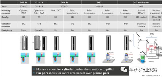
Figure 7: DRAM Roadmap
Another possibility is that the industry can develop non-volatile single-transistor (1T) DRAM devices. This is a capacitorless ferroelectric DRAM type device. But even with ferroelectrics, ferroelectric DRAM faces some challenges. "The problem is that it has some limitations. DRAM has almost unlimited endurance. This has been confirmed by ferroelectrics," said Imek's Van Houdt.
Imec is also pursuing ferroelectric device technology like 3D NAND. This technology, sometimes referred to as 3D FeNAND, uses a 3D NAND-based manufacturing process.
Van Houdt said: "It's low voltage and non-volatile. The power consumption is much lower, because it's a high-k material, it's faster, so it drives more current than NAND, which is NAND. Alternatives. Of course, it is almost impossible to replace NAND."
So, if it works, the device may be somewhere in the memory level pyramid of Figure 6. But technology will take five to ten years to enter the commercial market.
However, there are other problems. For example, in a paper by IEDM, SK Hynix, Lam, and others found that the actual switching speed of ferroelectric materials was slower than expected due to external problems.
SK Hynix, Lam and others have discovered a way to control the grain size of silicon-doped cerium oxide, which in turn increases the speed of the material set. "We have successfully demonstrated that Si:HfO2 is composed of controlled nanocrystals with FE properties of Ec~0.5MV / cm, which is half of ordinary Si:HfO2, and the domain switching speed is higher than that of ordinary grain size Si :HfO2 is three times faster."
What is an NC-FET?
Ferroelectric oxides have other uses. For some time, the University of California at Berkeley and other colleges have continued to study NC-FET, a next-generation logic transistor for 3nm or higher.
Like FeFET, NC-FET is not a new device. In NC-FETs, the gate stack in existing transistors is modified with ferroelectric oxide. The film thickness of the NC-FET is slightly different compared to the FeFET.
Mike Chudzik, senior director of Applied Materials' Transistor and Interconnect Group, said: "This is fun, just a simple ferroelectric exchange. I will arrange it along the FET tunnel."
The NC-FET has a subthreshold slope and is used in low power applications. It will compete more with tunneling field effect transistors (TFETs), a low-power transistor for 3 nanometers and above.
"Fundamentally, ferroelectric is like a voltage amplifier. You put a voltage, because it interacts, it will amplify the voltage. That's why you get this enhanced subthreshold slope," Chudzik said.
Based on this technology, the University of California, Berkeley Calibration is exploring the extension of today's FinFET and FD SOI technologies to 2nm. They called the new technology NC-finFET and NC-FD-SOI.
To be sure, the NC FET is still in its infancy. Chudzik said: "Although its research is full of possibilities and fun, there are still many unresolved issues."
But in the short term, FeFET is the most likely technology to achieve in these promising material combinations, which in turn may create a wave of R&D in this area. Otherwise, like other technologies, it will be left on the side of the road.
Wenzhou Langrun Electric Co.,Ltd , https://www.langrunele.com